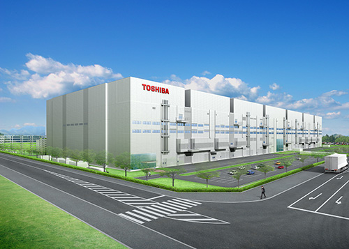
(iTers News) - Toshiba Corporation today broke ground to begin construction of Phase 2 of Fab 5, the company's state-of-the-art fabrication facility at its Yokkaichi chip making cluster for memory chip in Mie Prefecture.
Toshiba will expand Fab 5 to secure manufacturing space for 3D, or 3 dimension NAND flash memories that will be fabricated with a next generation of 3D chip making process technology. Construction will be completed in summer next year. The 3D NAND flash memory chip is a new generation of NAND chips that vertically stack transistors in a 3 dimension to cram more of them in a given silicon space. As the 3D NAND flash memory chip technology is very instrumental in lowering down the price of SSDs, or solid state disk to the level that match those of HDDs, chip makers like Samsung Electronics, Toshiba, and Intel are locking they horns in a battle for 3D NAND flash memory chips markets.
Samsung led the race, as the world's largest memory chip maker started volume production of the 3D V-NAND flash memory chips in early August.
Three fabs at the Yokkaichi Operations are producing NAND flash memories, including Fab 5 phase 1. Fab 5's construction was planned around two phases, the first of which went into operation in July 2011. As demand for NAND flash memory chips are expected to pick up in the years to come, mainly driven by smartphones, tablets, SSD for enterprise servers, Toshiba set out to build the 2nd phase of its Fab. 5 facility.
Outline of Fab 5


