(iTers News) - For years, graphene has been around, promising to replace silicon as a next generation of base materials for hyper-fast transistors, as it will be able to move back and forth electron 200 times as fast as silicon.
As the chip industry is especially nearing a deadend in scaling down the size of a silicon transistor as microscopic as below 10 nanometers, enormous efforts have been under way to etch graphehe-based transistors, but to no avail, because the nature of graphene is too semi-metallic to switch on and off current to create a series of 0s and 1s.
As recently as May 17, Samsung Advanced Institute of Technology, a hotbed of leading-edge technologies for Samsung Electronics, proved in theory it can be either conductor, or insulator, publishing its findings in the Journal Science. As far as graphene transistors are concerned, IBM is known to lead the development and commercialization project. Even if Samsung's graphen transistors are still on paper, the company seems to take a crucial first step to ride a next wave of technology breakthrough. To get more details, see below PR News
[sws_toggle1 title="PR News"> Samsung Advanced Institute of Technology, the core R&D incubator for Samsung Electronics, has developed a new transistor structure utilizing graphene, touted as the “miracle material.
” As published online in the journal Science on Thursday, 17th May, this research is regarded to have brought us one step closer to the development of transistors that can overcome the limits of conventional silicon.
Currently, semiconductor devices consist of billions of silicon transistors. To increase the performance of semiconductors (the speed of devices), the options have to been to either reduce the size of individual transistors to shorten the traveling distance of electrons, or to use a material with higher electron mobility which allows for faster electron velocity.
For the past 40 years, the industry has been increasing performance by reducing size. However, experts believe we are now nearing the potential limits of scaling down. Since graphene possesses electron mobility about 200 times greater than that of silicon, it has been considered a potential substitute.
Although one issue with graphene is that, unlike conventional semiconducting materials, current cannot be switched off because it is semi-metallic.
This has become the key issue in realizing graphene transistors. Both on and off flow of current is required in a transistor to represent “1” and “0” of digital signals.
Previous solutions and research have tried to convert graphene into a semi-conductor. However, this radically decreased the mobility of graphene, leading to skepticism over the feasibility of graphene transistors.
By re-engineering the basic operating principles of digital switches, Samsung Advanced Institute of Technology has developed a device that can switch off the current in graphene without degrading its mobility.
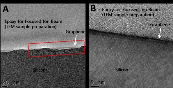
The demonstrated graphene-silicon Schottky barrier can switch current on or off by controlling the height of the barrier. The new device was named Barristor, after its barrier-controllable feature.
In addition, to expand the research into the possibility of logic device applications, the most basic logic gate (inverter) and logic circuits (half-adder) were fabricated, and basic operation (adding) was demonstrated. Samsung Advanced Institute of Technology owns 9 major patents related to the structure and the operating method of the Graphene Barristor.
As demonstrated in this research, the institute has solved the most difficult problem in graphene device research and has opened the door to new directions for future studies.
This breakthrough continues to keep Samsung Advanced Institute of Technology at the forefront of graphene-related industries.
*Schottky Barrier: Named after a German physicist Walter H Schottky, it is a potential (energy) barrier formed at a metal-semiconductor interface. It prevents an electric charge to flow from metal to silicon. Generally, metal-semiconductor junction would have fixed work function and Schottky barrier height, but as for graphene,
Schottky barrier height can be controlled through the work function. *Work Function: The minimum energy needed to take an electron out of material. *Inverter: A basic logic gate that converts a digital signal into the opposite level; “0” into “1” or vice versa. *Half-Adder: A logical circuit that performs addition of two binary digits. [/sws_toggle1]


