(iTers News) - As its migration to EUV, or extreme ultra violet lithography technology proves more challenging than expected, global chip-making industry hits a dead-end in scaling down its chip-processing technology below 10nm circuitry.
To break through the limit, chip makers are now struggling with a new groundbreaking way to fabricate transistors in a non-planar 3 dimensional structure. For example, SoC chip makers like Intel Corp. are now tinkering with a FinFET 3D transistor technology to reduce heat dissipation and current leakage that will further deteriorate as the width of the gate circuitry gets as narrow as 10nm and below.
On the other hand, NAND flash memory chip makers like Samsung Electronics and Toshiba Corp. are working on their respective 3D transistor cell structured-NAND flash memory chip technologies.
True enough, the chip-scaling technology is a measurement of how small a chip’s gate circuitry, or transistor is. As semiconductor industry’s mantra Moore’s Law implies, if the size of the transistor is cut in half, the density and the performance of a chip double, opening the way for cuts in half in costs.
Yet, everything has its own trade-off. The downside is that heat dissipation and current leakage increases in proportion to the shrinkage of the transistor size. As electron more often swerve out of the course between a source and a drain.
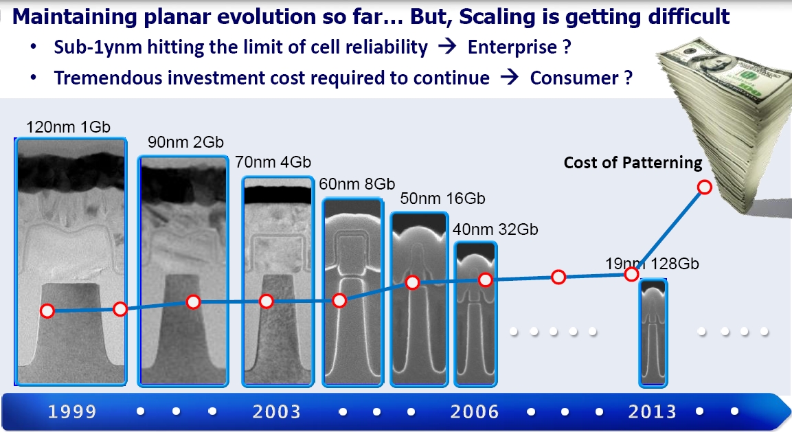
NAND flash memory chips are no esception to this heat dissipation. As the width of the chip circuitry gets narrower and narrower, the interference between cells gets intensified, aggravating electron leakages.
Especially when the circuitry gets down to 10nm and below, electrons start to bump against each other, making the 10nm circuitry NAND flash memory chip almost commercially unviable.
The commercial unavailability of the 10nm circuitry NAND flash memory chip technology comes as a shock to top-tier NAND flash memory chip makers like Samsung and Toshiba.
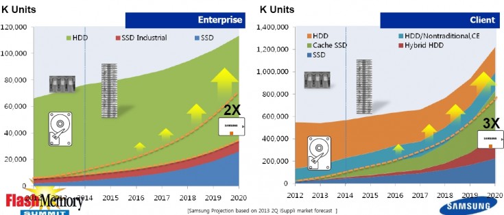
That’s because the nightmarish scenario suggests that NANAD flash memory chip-based SSDs, or solid state drives won’t undercut longtime rival HDDs on price at least for the time being, slowing down the penetration of SSDs into consumer electronics markets.
Stacking transistor cells vertically
That’s where the forte of Samsung Electronics’ 3D V-NAND chip-making technology comes in.
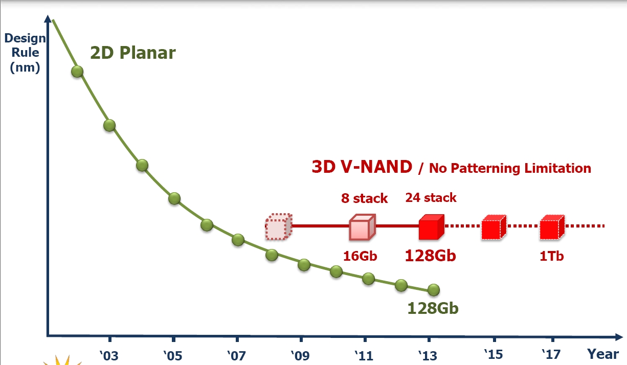
The 3D vertical cell-stacking chip making-technology can step up chip density by a magnitude of two times using current 20nm or 30nm chip circuitry processing technology without ramping up to a 10nm geometry technology.
On top of that, it can keep the cell to cell interference at the minimum and thus minimize electron leakages. .
The 3D vertical cell-stacking technology is a sort of disruptive technology that breaks away from conventional planar transistor technology. Samsung Electronics likens the vertically-stacking structure of the3D V-NAND chip to the world’s tallest towering 160-story Burj Khalifa skyscraper in Dubai.
Keys to the 3d vertical cell-stacking chip processing technology are Samsung‘s two homegrown indigenous technology breakthroughs – 3D CTF, or charge trap flash technology and vertical interconnect technology.
In the conventional planar NAND flash memory chip structure that is composed of a floating gate, a control gate and a channel, bit data of 1s and 0s, the most basic element of digital signals, are stored in its floating gate – a conductor - when voltage is cut off from a channel, as the cut-off traps electrons in the floating gate.
Repeats of write-on and-off of data out of the floating gate causes a short between a floating gate and a channel, souring the reliability of the NAND flash memory chips.
On the other hand, the CTF technology reorganizes the planar structure into a non-planar cylindrical structure, putting a channel gate at its core, then surrounding it with an insulator, and finally surrounding the insulator with a control gate. Electron, or electronic charges are stored on the insulator, which is made of silicon nitride film, not on a floating gate.
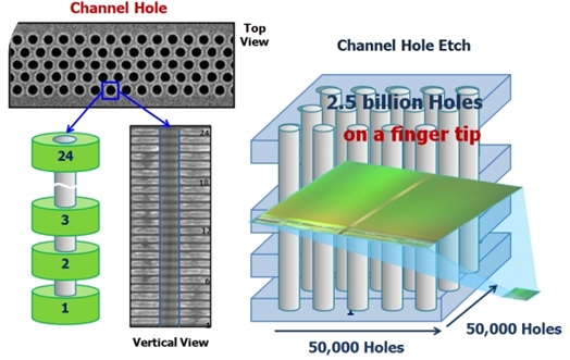
Then, Samsung stacked this single cylindrical layer of 3D CTF NAND flash cell on top of each other until it reaches 24 layers using special etching technology that connects the layers electronically by punching holes from the top to the bottom.
Xian, Chinese wafer- fab reday for mass rollouts 
Taking advantage of the two technology breakthroughs, Samsung developed a 128Gb MLC 3D V-NAND flash memory chip that is built with 24 layers of cells using an older 30nm-class process, and has been mass-producing them starting from early August.
The technology benefits are huge. Even though the 128Gb 3D V-NAND chip is processed with a relatively old 30nm-class design rule, the 128 Gb device carries two times more density in the same physical space than the planar structure 64Gb NAND flash chips of 20-nm class geometry. It also boasts better endurance and reliability. For example, the 128Gb 3D V-NAND can withstand 35,000 program per erase cycle, almost 10 times more than 3,000 program per erase cycle of today’s 20nm planar NAND flash chips.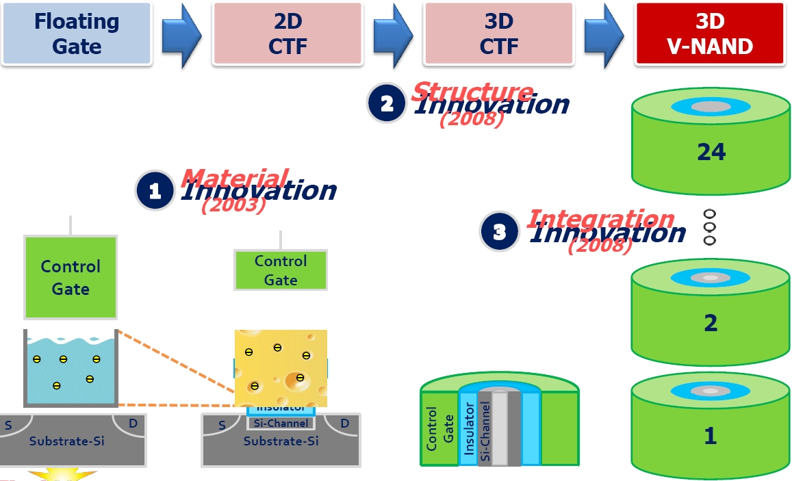
The new 3D V-NAND demonstrates two times reliability at the minimum, and a maximum 10 times higher reliability, too, compared with a conventional 20nm-class floating gate NAND flash memory chip. But, it also boasts twice as fast write performance.
“The new 3D V-NAND flash technology is the result of our employees’ years of efforts to push beyond conventional ways of thinking and pursue much more innovative approaches in overcoming limitations in the design of memory semiconductor technology,” said Jeong-Hyuk Choi, senior vice president, flash product & technology, Samsung Electronics. “Following the world’s first mass production of 3D Vertical NAND, we will continue to introduce 3D V-NAND products with improved performance and higher density, which will contribute to further growth of the global memory industry.”
Samsung also has built an enterprise SSD with the 3D V-NAND flash memory chips.
Meanwhile, rival Toshiba announced that it will start volume production of 3D NAND flash memory chips by mid-2014 when the 2nd phase construction projects of its Fab 5 in Yokkaichi facility in Mie, Japan is to be completed. Toshiba will use multilayered BiCS, or Bit-Cost Scalable manufacturing process for 3D NAND flash memory chips.
According to IHS iSuppli, the global NAND flash memory market is expected to growth at a CAGR of 11 % from US$23.6 billion in 2013 to reach approximately US $30.8 billion by 2016.