(iTers News) - Samsung Electronics and Toshiba Corp. are butting heads in the competition for a next generation of 3D Nand flash memory chips. The victory in the high-stakes game will give the winner a chance to seize control of fast-growing, multi-billion dollar SSD market.
A short of solid state drives, SSDs are a concentration of Nand flash memory chips seated together in a tiny printed circuit board. The silicon-based data storage technology is rapidly emerging as one of the most coveted market segments of global IT industry, as it is now threatening to replace decades-old HDD, or hard disk drive technology as a mainstream data storage technology for an array of computing system from server to desktop PCs to notebook and mobile PCs.
Compared with HDDs, SSDs consume less power, boasts far faster read and write time, and more importantly, can store more of data in a given space. Yet, it is still far costlier to produce, a big impediment against the rapid penetration of SSDs. The 3D, or 3 dimension Nand flash memory chip is rapidly emerging as a key technology-enabler to help cut costs of SDDs so steeply as to match those of HDDS, because it can store two times as much data as current planar structure transistor-based Nand flash memory chips.
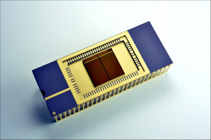
Vertically stacked
(Source : Samsung Electronics)
Samsung races one year ahead of Toshiba. The world’s largest memory chip maker said on August 6 that it has started mass-production of 128 Gb 3D V, or vertical Nand flash memory chips in what the chip maker said is the world’s first commercial roll-out.
Following Samsung’s lead, Toshiba said on the same day that it will join hands with SanDisk of the U.S. to build a joint-venture 3D Nand fabrication line as the second phase of its Fab 5 at its Yokkaichi facility in Mie, Japan. The two companies will invest 200 billion yen each to build the 400 billion yen wafer fabrication line to produce 3D Nand flash memory chips. Mass production is scheduled to start in the middle of 2014.
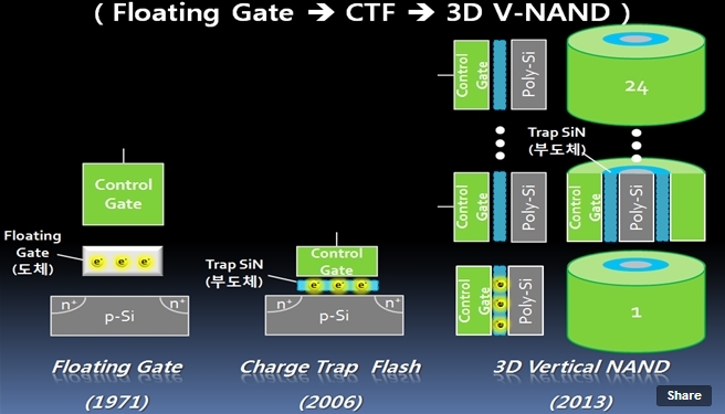
The conventional planar structure Nand flash memory chip transistor usually consists of one control gate and one channel gate as well as a in-between floating gate. Once a voltage is applied to the control gate, electron –the most basic element of digital signal data- gets trapped in a floating gate to keep data. Conversely, electron are relieved to erase, or rewrite data if a voltage is applied the channel.
High-stakes bet
On the other hand, Samsung’s 3D V-Nand flash chip transistor cell comes with a 24-layered cylindrical structure that vertically stacks 24 CFT, or charge trap flash cells. Each transistor consists of a control gate, a poly-silicon gate and an in-between insulating trap silicon nitride gate. Once a voltage is applied, the silicon nitride insulating layer traps electrons to store data. Samsung uses its indigenous vertical interconnect technology to vertically stack each cylindrical transistor. Electron moves up and down along the vertical hole to keep, or erase data.
The more transistors it stacks, the more storage capacity it can get. The technology difference translates into huge differences in performance –data read and write time as well as storage density per space. According to Samsung, the 3D V Nand flash memory chips, which were fabricate with a 20nm class design rule , can store double the density of its planar structure conventional Nand flash chip technology of a 10nm circuit geometry. It also boasts two times as fast read and write time.
The huge gains in the performance open the way for Samsung to cut production costs of SSDs, as the technology innovation allows the chip maker to pack two times as much storage capacity unit production costs. For example, the 3D V-Nand technology enables Samsung to cram 1 terabyte, TB storage capacity in a single piece of the 3D V-Nand flash memory chip 3 Nand in less than 5 years, according to Samsung.
To build one TB SSD Samsung SSD 840 Pro, Samsung crammed together 16 128Gb planar structure Nand flash memory chips, for example. The 1 TB Samsung SSD Pro now sells for about US$670. As is the case, Samsung’s 3D V-Nand flash memory chip technology will cut prices of the SSDs to cross over those of HDDs in the foreseeable future, promising to accelerate the replacement.
The 3D chip-making technology also enabled Samsung to break through the limits of the current geometry scaling down technology. True enough, the chip making industry is now confronting tough challenges in shrinking the Nand geometry technology below 10nm. That’s because the narrower the transistor cells get together, the more they interfere with each other. Prohibitively expensive EUV, or extreme ultra violet photo lithography equipment is also a hurdle, because the EUV equipment is very instrumental in going down below 10nm technology. Samsung’s commercial roll-out of the 3D V-Nand technology has paved way for doubling or tripling the storage capacity without moving beyond 10nm.
Break through the scaling limits
Once its chip-making facility in the city of Xian, China, Samsung also plans to churn out the 3D V-Nand flash memory chips there.
Toshiba Corp. has been working on the multi-layered 3D Nand flash memory chip technology using p-BiCS, or pipe-shaped Bit-Cost Scalable manufacturing process.
Unlike a 2D planar cell array, the 3D V NAND flash chip technology allows the chip maker to vertically stack 2D planar memory cells in a monolithic 3 dimensional structure.
Toshiba’s first roll-out of 3D Nand flash memory chip prototype went back to late 2012 when the chip maker unveiled a 16 layer prototype device using a 50nm geometry technology. Samples will be due out sometime in 2013. Toshiba’s p-BiCS technology arranges an array of Nand transistor cells in a U-shape.
According to IHS iSuppli, the global NAND flash memory market is expected to growth at a CAGR of 11 % from US$23.6 billion in 2013 to reach approximately US $30.8 billion by 2016. Yet, the prize is far bigger in the SSD market. Worldwide SSD shipments are set to rise to 83 million units this year, up from 39 million in 2012, according to market research firm iSuppli. Shipments are set to continue to rise 239 million units in 2016, about 40% of HDD market size. In terms of value, wolrdwide SSD market would hit US$ 17.2 billion in 2005
Video & Photos by Bae


