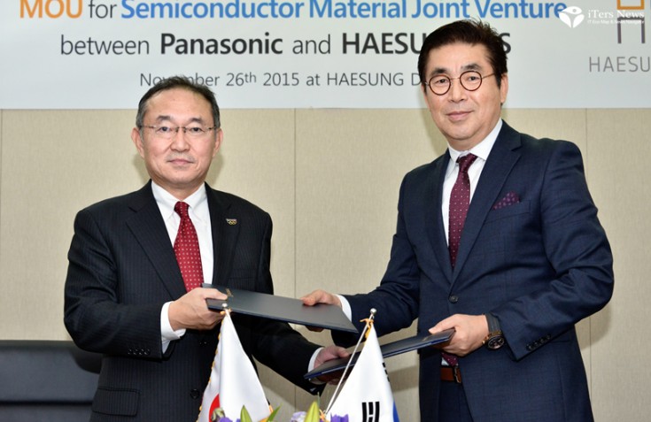
No term of the deal was available, including on specific amount of investment and information on how much stakes they will own respectively.
The possible win-win synergy effect was a perfect fit for the deal, as it enables the two partners to fill in the gaps in the production and technology portfolio.
The deal will enable Haesung DS, semiconductor packaging substrate and material maker, to gain access to its much-needed multi-layer BGA , or ball grid array substrate technology, helping to open up new business opportunities for mobile DRAM and SoC, or system on chip packaging market.
In return, Panasonic will be able to secure a strategically important production base in Korea not only to serve Koran memory chip makers, but also supply burgeoning Chinese chip makers, as neighboring China is on a spending spree to build mammoth chip fabrication facilities to produce a wide array of chips from SoC to memory chips. .
At a press conference held in Seoul on Nov.26 , Cho Don Yeup, CEO with Haesung, said, “ The MOU deal will allow us to expand our footprint into the multi-layer BGA substrate market like mobile DRAM ,and SoC BGA substrate packaging market.'
Once the joint-venture deal settled, Haesung DS plans to invest about 50 billion won to expand its production line.
Haesung DS is a substrate material and lead frame manufacturer for semiconductor chip packaging. The company spun off from Samsung Techwin, then , a subsidiary of Samsung group, or big conglomerate taking over the semiconductor chip packaging substrate and lead frame business and was recapitalized as a 100% independent company.


