(iTers News) - As chip industry’s technology migration to a next generation of photolithography technology EUV, extreme ultra violet light source is dragging on, chip makers are confronting increasingly tough challenges in getting down to 20nm and below 10nm nodes.
To keep up with the chip industry’s decades-old mantra Moore’s Law, an observation that the number of transistors doubles every 18 to 24 months, they are turning to alternatives like 3D FinFET chip architecture, multi-patterned chip design and 3D TSV packaging technology.
The mass rollout of these alternative technologies has more to do with innovations in raw materials than equipment and chip-processing technology. That opens up new market opportunities for raw material makers as well test and measuring equipment makers. But it also presents challenges.
“With new process and new integration needs, process technology and material requirements are becoming more complex and costlier. And continued advancement in silicon device performances is more challenging, as scaling continues to finer geometry. As chip scaling technology continues to get down below 10 and possibly 7nm node, semiconductor industry is looking beyond CMOS to address challenges for further device performances. New device architecture and materials will advance device performances,” said Denny McGuirk, president and CEO with SEMI, an industry lobbying group representing semiconductor equipment and material makers across the world. 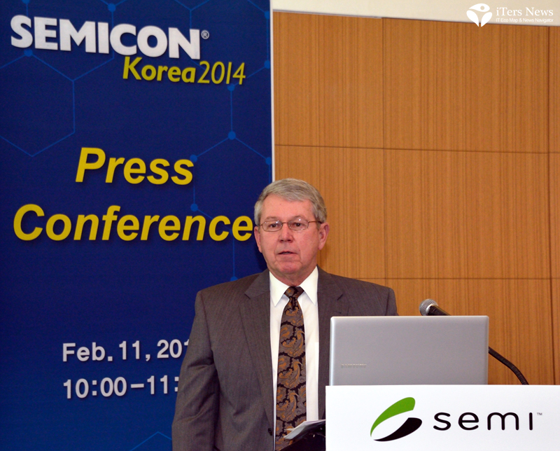
Added he, “EUV, extreme ultra violet and multi-patterning technology will be used at the leading edge. New packaging schemes such as 3D chip architecture and 3D packaging architecture, through Silicon Via or TSV will deliver further integration for the performances within small for factor. Those industries need cost-effective approaches in ramping up to these technologies and need to address issues around thermal performances electrical testing and packaging reliability.
As such technical challenges are too complex for a single company to tackle, he recommended that chip makers, semiconductor equipment makers, raw material makers alike work together to find right solutions.
One prime example is Samsung Electronics’ 3D V-NANA flash memory technology. Unlike a conventional planar NAND flash memory chips that stores a string of 1s and 0s in a conductive floating gate, the 3-dimenstional vertically-stacked NAND flash memory chip charge and discharge digital signals or electrons into a holding chamber of a non-conductive layer of flash composed silicon nitride in what’s called as charge trap flash, or CTF. Forming a non-conductive insulating gate requires innovation in chemistry like different chemical compound and formulation, however. 
The mass-rollout of multi-patterning chip design technology is challenging, too. The multi-patterning technology is to expose ArF immersion light source twice, or four-times to pattern multiple lines between already traced circuitry lines. The upshot is that the width of the circuitry line gets thinner, but becomes very fragile, getting vulnerable to defect.
To tackle that issue, chip makers and raw material makers alike are working on advanced plating materials and advanced barrier materials like cobalt and ruthenium.
“As chip makers are hitting limits in the photolithography chip technology, they are turning to double and quadruple patterning technology. Accordingly, we are more focusing on advanced materials like precursor deposition materials,” said Steve Jang, country manager in Korea with ATMI Inc.
ATMI is Tempe, Arizona, U.S.-based supplier of ion implantation and doping materials and implant gas delivery system like safety material delivery canisters. The ion-doping or implantation process is crucial part of the front-end chip making processes to implant various ions like baron and phosphor to create N-and P-type transistors in a complimentary for in what’ called as complementary metal oxide semiconductor CMOS process.
The ramp-up to 3D FinFET transistor technology also requires innovations in equipment tools and materials.
“As we move toward technology known as 3D FinFET transistor architecture, the device is getting so small. The direction field-on is very near the surface. This requires differentiations from the past beam-line light doping. Right now, we are working on a very large product line to enable this particular tool with our doping, “ added Jang with ATMI.
Lasertec Co., Ltd of Japan is also scrambling to turn the technology challenge to its advantage. The supplier of laser-based inspection equipment for patterned photo masks is seeing huge market opportunities where others face risks.
“As chip makers are ramping up to 20nm and below node, they are increasingly concerned about the defect, because it will reduce yield-the ratio of sellable item out of total production. The more concerned they are, the more of high–resolution inspection equipment they want to install,” said Lim Choon Gab, leader of sales group with Lasertec Korea Corporation.
The Japanese chip inspection maker is also logging growing orders for 3D TSV packaging inspection equipment.
True enough, the chip integration technology is getting more and more important, as chip maker are struggling to keep pace with the growing system requirements for smaller, but a lot powerful and faster and power-thriftier chips.
What matters the most in the fast-growing mobile applications are tiny form factors, longer battery life, and powerful system performances.
The system requirements in turn call for semiconductor chips to get far smaller, much power-thriftier, and faster in processing data
“Market opportunities associated with mobility and connectivity trend are represented by the rapidly increasing number of personal mobile electronics. I am sure we not only have one, or two, three, and sometimes four different mobile devices that we use on a daily basis.” Denny McGuirk, president and CEO with SEMI
He predicts that worldwide semiconductor chip market would be better off in 2014, mainly powered by soaring demand for mobile devices. He added, “The outlook for the fiscal 2014 generally looks more positive in terms of semiconductor sales and investments. The 2014 will be the first year for the communications IC spending to pass the PC IC spending,”
As the industry is struggling to tackle these challenges, SEMI forecasts that global capital equipment revenue would jump from US$32 billion in 2013 to US$40 billion in 2014. Worldwide spending on raw materials will also rise from US$44 billion in 2013 to US$45 billion in 2014.
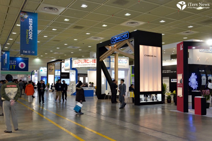
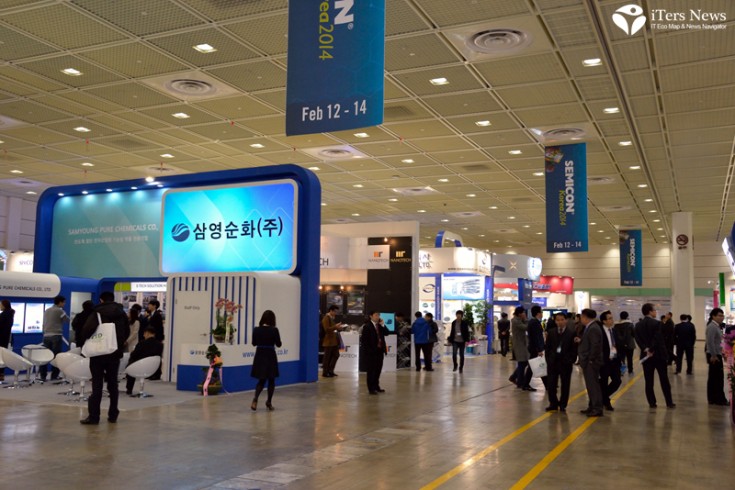
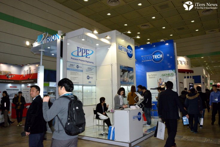
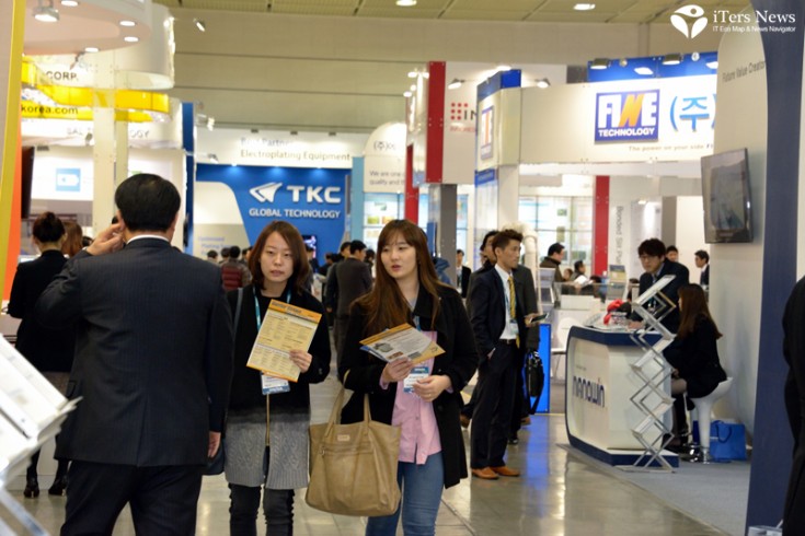
(Photos and Videos by JH Bae)