(iTers News) - As global consumer electronics and IT titans are in a desperate lookout for a next wave of growth engines to pump up new vigor into long-idle IT and consumer electronics markets, a flurry of new technology standards are in the offing, promising to create potentially huge new market opportunities.
That is where the forte of FPGA, or field programmable gate array starts in. The inherent nature of the memory cell-based FPGA chips is its programmability that can allow chips makers and system makers alike to reprogram them not only to differentiate their products, but also meet constant changes in the technology standards, or communications network protocols.
More importantly, FPGAs better serve relatively low volume applications than ASICs, as they are programmable, or configurable, depending applications. As with the case, FPGAs have been widely used with some prototyping projects for applications that usually start with low initial volume.
Today’s buzzword 4K UHD TVs are typical of those applications that promise huge demand for the long terms, but have a long way to go before they hit critical mass.
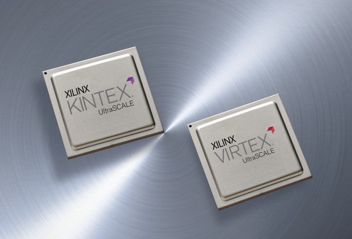
To capitalize on the trend, world’s largest FPGA chip maker Xilinx, Inc. has built the newest version of its mid-end Kintex and high-end Virtex FPGA chip solutions around its 20nm All Programmable UltraScale architecture.
The 20nm All Programmable UltraScale architecture is the first ASIC-class FPGAs that incorporate some of ASIC chip design scheme and methodologies. Not only do they perform as powerful as ASICs, but also almost match them in power consumption.

Built on the 20nm UltraScale architecture, these two FPGA families deliver a next generation of routing, ASIC-like clocking, and enhancements to logic and fabric to eliminate interconnect bottlenecks while supporting consistent device utilization of more than 90% without performance degradation.
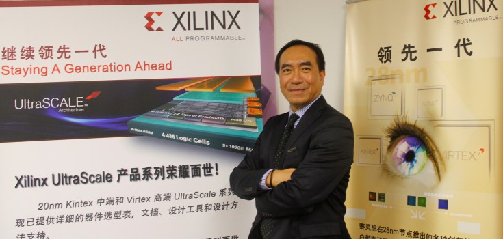
"What we have done with the previous generation of 28nm design architecture, which is very successful today is that this will not likely disappear in 2 to 3 years. We will continue to see many and many customers use it. That provides very optimum performance, price and power, and also SoC integration was made. We do see some areas, especially in some very high-end smart networks and machine vision type of applications, we realized that we need to have a different architecture to complement what we have done with the 28nm architecture, " said Vincent Tong, senior vice president with Xilinx, Inc.
"That's why we have today a 20nm UltraScale FPGAs, which are really useful for complementing the 28nm architecture on the high performance applications space. This 20nm architecture is not only to complement the 28nm FPGA, but also set a stage for a future 16nm architecture, which is a FinFET 3D transistor, multi-processing power and tons of memory cells. With this 20nm architecture, FPGA can become really ASIC-class, going into ASIC-class type of applications. That means a lot for Xilinx, because all of you know how big the ASIC business is. More importantly, we have now the 20nm UltraScale product portfolio and started to ship them for customers," added he.
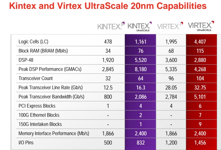
For example, the new Kintex UltraScale FPGAs deliver up to 1.16M logic cells, 5,520 optimized DSP slices, 76 Mbits of BRAM, 16.3Gbps backplane-capable transceivers, PCIe Gen3 hard blocks, integrated 100Gb/s Ethernet MAC and 150Gb/s Interlaken IP Cores, and DDR4 memory interfaces.
The Kintex FPGA family has already secured a dominant market position in the market segements using the previous 28nm architecture.
The 20nm Kintex UltraScale devices are designed to continue leadership in this category to meet requirements for the growing number of key applications including 8K/4K ultra definition displays, 256-channel Ultrasound, 8X8 Mixed Mode LTE and WCDMA radio with smart beamforming, 100G Traffic Management/NIC, and DOCSIS 3.1 CMTS equipment.
Setting new industry standards, the newest version of the Virtex UltraScale devices provide unprecedented levels of performance, system integration and bandwidth on a single chip. The largest family member delivers 4.4M logic cells, 1,456 user I/Os, 48 x 16.3 Gb/s backplane-capable transceivers and 89 Mbits of Block RAM, breaking previous records by more than doubling Xilinx’s industry’s highest capacity Virtex-7 2000T device and delivering a staggering 50M equivalent ASIC gates.
Virtex UltraScale devices include 28Gb/s backplane-capable and 33Gb/s chip-to-optics transceivers, in addition to integrated PCIe Gen3, 100Gb/s Ethernet MAC and 150Gb/s Interlaken IP cores, and DDR4 memory interfaces to support multi-hundred gigabit-per-second levels of system performance with smart processing at full line rates.
The system performance and capacity delivered with the Virtex UltraScale family makes these devices the logical choice for the most challenging applications such as single chip 400G MuxSAR, 400G Transponder, 400G MAC-to-Interlaken bridge, Emulation and Prototyping,
Those two 20nm families come coupled with the Vivado ASIC-strength design suite and UltraFast design methodology to allow Xilinx's customers to easily implement their product concept or idea and own IPs into their real products to differentiate them from competition. "with all these hardware features like embedded processors, FPGAs and memory, we have to have software and tools to allow our customers to implement their IPs to deliver smart system with highest level integration and lowest cost and highest performances," stressed Vincent Tong.
Ip


