(iTers News) - Following on the heel of its roll-out of 28nm All Programmable FPGA solution in 2012, Xilinx Inc. has successfully taped out a new 20nm UltraScale FPGA architecture that will form the basis of all of its 20nm mid-and high-end FPGA solutions. The tape-out of the 20nm UltraScale architecture represents Xilinx’s ambition to extend its break into new applications markets that ASICs, or applications-specific integrated chips historically have served, but still remain relatively lower in volume, compared with other ASIC applications.
With the 28nm FPGAs, Xilinx has already secured about 40% of its design wins from telecommunications sectors that used to be the historical stronghold of ASIC designs, according to the compnay .
True enough, ASICs usually outdo FPGAs in power consumption, costs, and performance, but require big enough volume to justify prohibitively exorbitant investments in chip designing and fabrication.
A short for field programmable gate arrays, meanwhile, FPGAs underperform ASICs, consume more power, and cost a lot more dearly, but can be reprogrammed so that they are flexible in meeting constant changes in technology standards, or communications and network protocols.
ASIC outperform FPGAs, but not flexible
More importantly, FPGAs better serve relatively lower volume application than ASICs, which work on only one specific application, as they are programmable and configurable, depending various different applications. As is the case, FPGAs have been widely used with some prototyping projects for applications that usually start with low initial volume, but can eventually deliver on high volume. For example, today’s buzzword 4K ultra HD TVs is typical of the applications, promising to create huge demand, but have a long way to go before they reach critical mass.
That’s where the forte of FPGAs comes in, because initial demand for 4K TVs won’t grow big enough and fast enough to justify design and chip-fabrication costs of ASICs.
Once hardwired, ASICs won’t be reprogrammed, either, failing to keep pace with possible changes in the 4K standard or algorithm.
Where FPGAs prevail
As chip design and fabrication technology rapidly evolves, however, FPGAS are now threatening to challenge ASICs in performance and power consumption to break into some yet untapped, relatively low volume segments of traditional ASIC application markets.
These applications are especially all about a next generation smart systems that require ASIC-like performances in packet processing, data flow, and I/O and memory bandwidth, but can’t generate as big volume as TV, mobile phones, and game consoles.
That’s where Xilinx’s new 20nm UltraScale architecture is zeroing in on.
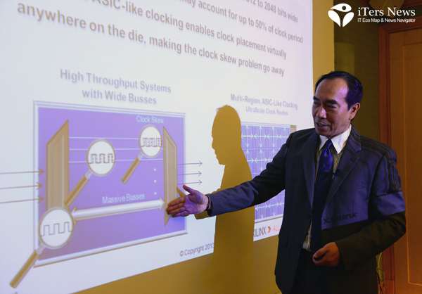
(Photo Caption : Vincent Tong, Senior Vice President, Xilinx Inc. )
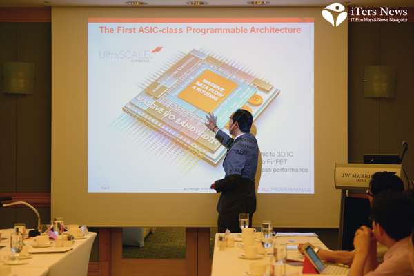
The UltraScale architecture is the first ASIC-class FPGAs that incorporate some of ASIC chip design scheme and methodologies, performing as powerful as ASICs, and almost matches them in power consumption, according to Vincent Tong, senior vice president with Xilinx Inc.
For example, the 20nm UltraScale architecture has the same dedicated memory IO lines that ASICs implement to directly fetch up data into its silicon die rather than scanning and routing all memory cells to find the right memory address. Available in the predecessor 28nm FPGAs, the dedicated IO bus lines help ease up data congestion, or bottleneck in massive data flow between memory system and FPGAs.
“In last generation, we have solved very, very big problem for our customers which is connection, the connectivity here. So, we have many very fast IOs so that people can put a lot of into the silicon. In many ways, this actually equals, or is better than ASIC chip can do with IOs and transceivers Challenges here you have massive data flow from outside into the device, so that there is a lot of congestion in the FPGA architecture before,” said SVP Vincent Tong.
He said that Xilinx has improved its UltraScale FPGA architecture’s IO throughput speed up to 56Gbps using this ASIS-like dedicated memory interface schemes.
Technology innovations don’t stop there. To achieve ASIC-class performances, FPGA chip makers like Xilinx have been exponentially implementing a lot of logic elements, or IPs on their silicon. The challenge facing the FPGA industry in doing so, however, is how to not only increase the number of tracks inside the FPGAs to accelerate data flow-in and-out, but also streamline the interconnection between logic gates.
Smart routing
FPGA’s traditional way of data interconnections between logic gates have data in one logic gate move around all nearby other logic gates to reach another faraway target lgic gate. Unfortunately, however, the roundabout creates data latency, or delays, resulting in deterioration in overall performances.
To tackle the challenge, Xilinx has again implemented ASIC-like smart data routing scheme to speed up data interconnections between logic elements by setting up direct data path between one logic gate and the other far way logic gate using a 3D transistor IC design scheme.
“We are looking into what ASIC design need, and we are putting the design into our next generation of FPGAs. In the last generation, we have done a lot putting data on a chip, Now, the bottleneck suddenly becomes interconnect within the FPGA. That’s why we need to apply some ASIC techniques into the full programmable architecture,“ stressed SVP Vincent Tong.
As the FPGA industry moves from one generation to the other, according to him, it has provided exponential capability to get more of IPs into the chips. Once these IPs implemented on the chips, however, the challenge is all about how to get those data through the chip to do a lot of processing like data analysis and decision-making.
“In order to increase the logic contents, the No. 1 thing we have done here is to increase the track within the logic. No matter how much we increased the track here, however, the problem is that the ratio is getting worse. That means, for example, to send signals from one area to the other far away area, signals have to go through a lot of programmable elements, causing a lot of congestions. The very simple thing we have to do is that just like ASICs, we will create direct connection between them. In reality, this block looks like sitting next to the other block,” added he.
Xilinx has also tackled what’s known as FPGA’s biggest challenge yet - clocking skew – by implementing multi-region ASIC-like clock schemes to increase clock sources. Traditional FPGA used to have very few clock sources, but the UltraScale architecture has implemented many clock sources to perform ASIC-like high performance functionality.
Parallel multiplexing execution algorithm is another ASIC technology that the UltraScale architecture has implemented on its die. It helps to speed up the operation of DSP blocks. On top of that, the UltraScale architecture distinguishes itself from other FPGA architecture in addressing memory cells. Unlike traditional FPGAs that have to rout all memory cells to address a certain memory location, the UltraScale can directly address each of memory cells by implementing ASIC-like hardened block RAM schemes in what the chip maker calls as high-fast memory cascading. It leads to removals of bottlenecks in DSP and packet processing, while helps avoid uses of additional on-chip routing or logic resources.
Rich in clocking source
In what the FPGA chip maker calls another ASIC-like design methodology, Xilinx has also hard-wired as many mature legacy logic blocks as possible. For example, it has hardened such legacy IP blocks as PCIe core IP, 10/100G Ethernet, and Interlaken blocks. By doing so, it has come to not reduce data latency, but also allocate many programmable logic and routing resources available for other functionality.
All combined, those ASIC-like design methodologies eventually have helped to significantly reduce one of FPGA’s biggest Achilles Hills -power coumsption.
According to Xilinx, the 20nm process technology alone helped reduce the static power consumption by 25% to up to 35%, compared with the predecessor 28nm geometry technology. In addition, the hardened IP block, clock gating, hardwired memory cascading, and newly optimized transceiver architectures have all combined to cut back power consumption.
The 20nm UltraScale architecture will form the basis platform for its Virtex and Kintex FPGA and 3D IC families, which are now built with the 28nm process, as well as its future Zynq UltraScale All Programmable SoCs.
With the first rollout of the UltraScale architecture chip scheduled for the fourth quarter of the fiscal 2013, Xilinx is setting its sights on such applications markets as 400G OTN switching with intelligent packet processing and traffic management, 4X4 Mixed Mode LTE and WCDMA Radio with smart beamforming, 4K2K and 8K displays, super high vision processing, 256-channel Ultrasound, and ASIC prototyping.
Yet, the debut of the ASIC-class UltraScale architecture-based FPGA chips is not necessarily to say that Xilinx will attempt to replace all ASIC solutions with the UltraScale FPGAs.
“These high performance smart system applications can be now addressed by Virtex and Kintex UltraScale architectures. But, they (ASICs) always have some advantages in performance and power, and most importantly, they need huge volume. They also have cost- advantages. ASIC are very expensive unless they have volume. If I say high volume, that means cell phone-type high volume and PC and tablet-type high volume. If you look at these applications, none of these will be able to deliver that high volume. Where do they go? They need performances of ASICs. They need to have some power savings of ASIC. They don’t need volume,” said Vincent Tong.
ASICs also have difficulties in keeping up with the constant changes in algorithm and standards on these applications, because they have fixed blocks.
Take on traditonal ASIC market
“That’s why we believe the UltraScale architecture would take on these applications,” he added.
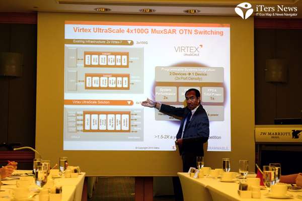
The 400G OTN, or optical transport network switching is one example of how FPGAs undercut ASICs on costs unless it can generate big enough volume to amortize huge investment in ASIC designs.
According to Xilinx, its current Virtex 7 FPGAs can’t afford to serve that application, because it is still very short on performance and power consumption, only serving 200G OTN application. When it comes to power consumption and performance, however, the 20nm UltraScale architecture can rival ASICs to take on the this application, because they have cost advantages.
“With the 20nm UltraScale architecture, they are converting a lot of originally ASIC designs into FPGAs. So, we definitely know where the trend is going,” SVP Vincent Tong emphasized.
Photos & Videos by JH Bae


