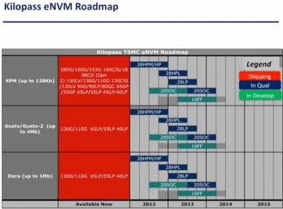
The hardwire implementation of its NVM IP on a silicon die for a 20nm geometry SOC proves commercially viable.

The successful implementation will open up huge new market opportunities for Kilopass to toss up, as SOC chip makers will welcome with open arms as a cheaper replacement to on-chip SRAM and external EEPROM that takes up extra cost, power, and real estate on a board layout.
The IP provider announced that TSMC, a Taiwanese foundry chipmaker TSMC has successfully tested the implement of its antifuse NVM technology on a 20nm node SOC solution, showing its manufacturability, process control tolerance and cell programming characteristics got validated.

"Our NVM IP cell arrays are designed to be compatible with Double Patterning Technology (DPT). Our successful experience on two generations of high-k metal gate processes gave us the know-how to successfully scale our NVM IP," added he.
As with the 28nm process experience, Kilopass NVM IP in the 20nm process achieved an operating window of over three decades between programmed and un-programmed cells. The Kilopass NVM IP also demonstrated excellent programmed cell current under different programming conditions.
"Enabling our NVM IP on the latest TSMC 20nm gives us the lead position providing antifuse NVM IP," said Linh Hong, vice president of sales and marketing at Kilopass.
"Next generation SoC designs-network processors, baseband, application processors-that previously relied on external serial EEPROM and on-chip shadow SRAM to contain boot code, configuration data, and security keys are seeking to eliminate this combination in 20nm designs. Our NVM IP provides a more cost effective solution that will occupy the equivalent space of the on-chip shadow SRAM and most importantly will be available on the new 20nm TSMC process node. It will also eliminate the cost, power, and pads taken up by the external serial EEPROM,." added he.
Kilopass NVM IP is now available for customer designs.
(Featured image : Harry Luan, CTO with Kilopass Technologies )
Credit for video clips and photos: Kilopass)

