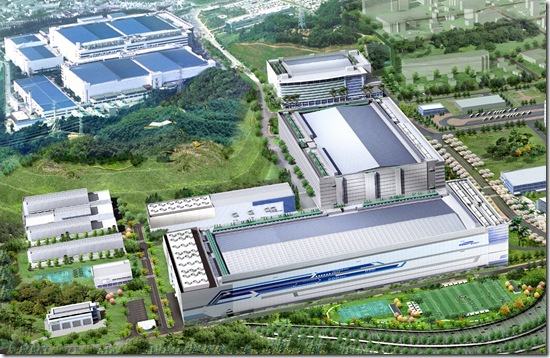
(iTers News) – Samsung Electronics Co., Ltd. plans to build a new 300 wafer fabrication facility in China to produce NAND flash memory chips in what the chip maker said would be its first Chinese front-end chip-making facility ever.
The global memory chip leader is now seeking the Korean government permission for the overseas facility investment plan, the prerequisite for companies in such hi-tech areas as semiconductor and TFT-LCDs to undergo to invest in rival countries that would come as a threat to the home-grown industry’s future vitality.
It’s still unknown and undecided where to build the 300mm wader facility, the company said.
According to local vernacular daily reports, Samsung plans to invest about US$4 billion to build the fab facility, which will come on line by 2013 to mainly roll out NAND flash memory chips of 20nm geometry. NAND flash memory chips are crucial data storage devices in every mobile gadget from smartphones to tablet PCs .
Samsungs has been operating a back-end test & assembly facility for memory products in Suzhou, China for more than 10 years, but has forgone investing in front-end wafer process facility.
Exploding demand for NAND memory chips in China was irresistible lures. China is now the world’s largest and fastest-growing mobile phone market, guzzling every nuts and bolts to build mobile phones and smartphones.
Samsung’s backyard archrival Hynix Semiconductor is better poised to supply soaring Chinese demand, as the chipmaker has been operating a joint-venture 300mm wafer fabrication facility in Wuxi, China to produce NAND flash memory chips.
Market research firm Gartner Inc. expects global NAND flash markets to grow by 20.6% in 2011 to reach US$25 billion. Looking forward, the market is forecast to grow 14% year-on-year in each of 2012 and 2013 to hit US$28.7 billion and US$32.7 billion, respectively.
Samsung is the world’s largest NAND flash memory chip maker, taking up about 40% share.
The chip maker recently got a new 300mm wafer fab called Line-16 up and running in the Hwasung wafer facilities in the city of Hwasung, 60km southwest away from capital Seoul -home to its memory chip production.


