(iTers News) - The semiconductor industry’s mantra Moore’s Law hits a snag in delivering on its promise that the industry would double the number of transistors every 18 or 24 months, facing the toughest challenge ever in ramping up to a finer chip processing technology.
As the industry is now struggling to go below a 20 nanometer and below chip processing technology, for example, it suffers from slowdowns in the chip performance gain as well as difficulties in containing increases in heat generation and power consumption.
That’s because it is increasingly difficult to trace and pattern transistors of which geometry is as thin as 20nm and 10nm without compromising power consumption. So is it to pack two times more transistors into a given silicon footprint every 18 or 24 months.
This technology challenge helps explain why chip giants like Intel Corp. are now turning to a 3D FinFET chip-making technology for future generations of SoCs, as they are scrambling to fabricate chips of as thin geometry as 20nm and 10nm.
NAND flash memory chip makers are no exception. To tackle technology hurdles in reducing costs, doubling chip density, and improving reliability, NIAND flash chip makers are working on a 3D NAND chip technology, too.
Leading their migration to the 3D chip technology is Samsung Electronics that is already mass-producing 3D V-NAND flash memory chips.
“You need another new approach to build the foundation for the future generation of NAND flash memory chips. Disruptive technology is required to satisfy capacity, cost, and reliability requirements,” said Dr. Kye-Hyun, Kyung, senior vice president of flash design team with Samsung Electronics Co., Ltd.
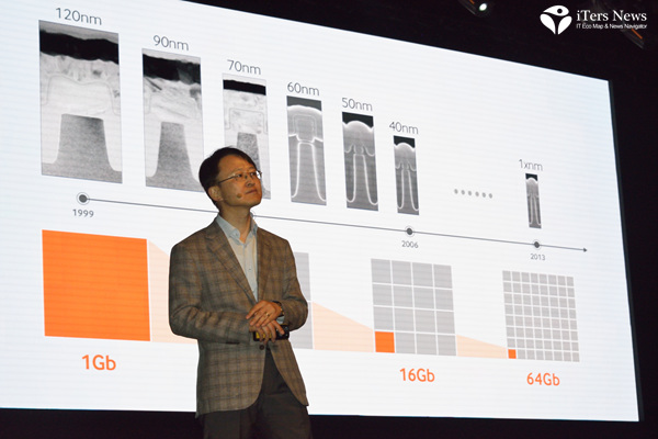
Added he, “The benefit of reducing the cell size was vast. In 1999, we only produced 1Gb NAND flash memory chips with a 120nm design rule technology. But, now with the 10nm-class chip processing technology, we can fit 64 times more cells into a same area to put 64Gbs of data (compared with the 120nm technology). Every time, we shrink the cell size, however, we already face technical challenges. We need to develop a design technology to prevent the cell to cell interference. And we should find light source for photolithography process.”
As the geometry of the NAND flash memory chips got below 20nm, according to Dr. Kyung, it started to get increasingly difficult to control the cell-to-cell interference. The ramp-up to the 10nm processing technology also required prohibitively expensive investment costs on new light source equipment for photolithography process like EUV, or extreme ultra violet machine, leading to hefty increases in the chip production costs. It takes still a couple of more years before the EUV equipment gets fully commercialized, too.
The width of the chip circuitry depends on the wavelength of the light source. The EUV is the next generation of light source for patterning the 10nm-class chip circuitry, because its wavelength is far shorter than current ArF immersion light source technology.
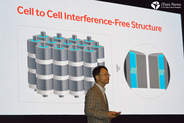
The cell-to-cell interference refers to a phenomenon that one cell affects the behavior of another adjacent cell in what’s called as a coupling effect, resulting in data corruption.
The narrower the distance between cells gets, the stronger the interference gets, corrupting more of data.
Bedeviled by these two major technology challenges, NAND flash memory chip makers hit a dead-end in further increasing the density of a chip. For example, the 128Gbs are the maximum chip density that a NAND flash memory chip of a 10nm-class circuitry can implement.
To break through the technology bottleneck, Samsung broke new grounds in three key areas; material engineering, cell interconnection, and chip structure.
Unlike current NAND flash memory chips that are built with a 2D planar structure. Samsung stacked cells over cells horizontally in a 3 dimensional structure to fabricate a 3D V-NAND flash memory chip.
The 3D chip structure paved the way for Samsung to exponentially increase the density of the NAND flash memory chips, enabling it to break through a current ceiling of 128Gb density with no recourse to a far finer design rule technology..
Using a 20nm-class design rule technology, for example, Samsung packed as many densities in a 3D structure as the chip maker did in 2D planar with a 10nm-class manufacturing process.
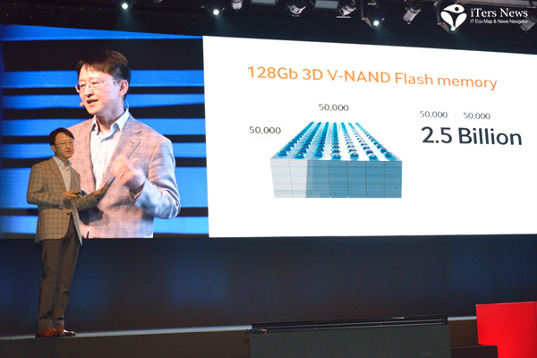
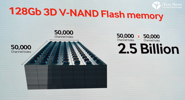
Samsung is now fabricating 24-layer and 32-layer 128Gb 3D V-NAND flash memory chips in high volume using a 20nm class-design rule stacking cells on the top of each other up to 24 and 32 layers, respectively.
Innovations in material science also helped Samsung to eliminate the cell-to-cell interferences. Consisting of a floating gate a channel gate, and a control gate, the 2D planar structure NAND flash memory cell stores data in a conductive floating gate, writing and reading it out of the gate.
On the other hand, Samsung’s 3D V-NAND flash memory chip stores data, or electronic charge on a non-conductive insulator using what’s called as a charge trap flash, or CTF technology and then surrounds it with a control gate.
“Our research team had been working on a way to build a cell-to-cell interference-free chip structure, while scrambling to develop a technology to stack more capacity in a given silicon footprint with a larger design rule,” said DR. Kyung of Samsung.
True enough, Samsung’s CTF technology is a new breed of groundbreaking memory chip technology that uses a non-conductive insulator as a data storage circuitry instead of a conductive floating gate. Etching the insulator circuitry on a silicon wafer required new chemical compound that is different from those used for a conductive floating gate.
Unlike a floating gate where data or electronic charge easily moves in and out, the insulator layer tightly keeps data inside, steering clear of coupling effect and thus cell to cell interference phenomenon.
“As a control gate covers an insulator, there is no cell to cell interference in the 3D V-NAND. In other words, the insulator prevents signal noises, there is no cell to cell interference,” said Dr. Kyung.
To vertically string together cells over cells, Samsung also developed what’s called as channel hole technology, a sort of cell interconnection technology that vertically interconnect layer over layers of cells by punching holes all the way through bottom to top. The vertical interconnection technology allowed Samsung to stack up to 32 layers of cells vertically.
All combined, those technology breakthroughs translate in tremendous gains in chip density performance, reliability, endurance, and power consumption.
For one thing, the 3D NAD flash chip technology laid the foundation for Samsung to exponentially increase the chip density. By 2017, Samsung bets that it will be able to fabricate 1 tera bit 3D V-NAND flash memory chip.
As it comes with no software algorithm to verify and correct cell-to-cell interference, it can also write and read data about two times faster than a 2D planar NAND flash memory chip. It also consumes 46% less power, as it doesn’t need to decode the software algorithm.
Longer endurance is another edge. Endurance is a measure of how many times a NAND flash memory chip can write data into cells. As the 3D V-NAND writes data into an insulator, which is more resistant to data wear-out or corruption, it boasts 2 to 10 times more endurance.

These improvements come at a crucial time when NAND flash memory chip-based SSD or solid state drives are increasingly replacing conventional HDDs as a mass-storage device for PCs and data center serve computers.
Samsung bets that mass-production of 3D NAND flash memory chips will likely accelerate the replacements, as it would help greatly reduce costs.
Coming complete with NAND flash memory chips, memory controllers, and a firmware, SSDs far outperform HDDs in data reading and writing speed, but its unit cost per byte is still more expensive than that of HDDs, although there have been dramatic cut-downs in the byte-per-unit price.
For example, the unit price-per-byte of SSDs hovered above US$15 in 2006 when single level cell, or SLC NAND flash memory chip-based SSDs were first released. In 2008, the unit price dropped to US$5.1 per byte, as the industry rolled out world‘s first MLC or multi-level cell NAND flash memory chip-based SSDs.
In 2012 when a 512GB SDD rolled off the production line, it broke a barrier of US$1 per byte, gaining watershed momentums to replace HDDs in PC and other consumer electronics markets.
“Think of data center, and stacks of HDDs are replaced by SSDs. NAND flash memory chip is ubiquitous. It is everywhere and is now an integral part of virtually every consumer CE device out there making a significant inroad into data center and server infrastructure,” Jim Elliott, vice president of memory marketing with Samsung Electronics.
According to him, SSD market will grow 30% in 2014 and continue to grow at CAGR 25% to hit US$20 billion in 2017.
As the rapid proliferation of connected devices like smart phones and tablet PCs would drive explosions in the data traffic, he expects data center would become more storage-hungry, fueling explosive demand for SSDs.
“Facebook logs more than 9 billion page views per day, while more than 500 million tweets are being uploaded per day. Think of YouTube. More videos are uploaded to YouTube in one month than major U.S. broadcasting networks created in 60 years. That is the pace of the change the industry is experiencing right now,” added Jim Elliott.