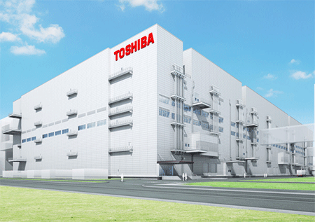
(iTers News) - Toshiba Corporation has telegraphed its strong intention to compete head-on-head with Samsung Electronics for control of 3D NAND flash memory chip market. The Japanese memory chip maker said today that it would recalibrate its Yokkaichi NAND flash memory wafer fabrication facility in Mie prefecture, Japan to replace it with a new fab for 3D NAND flash memory production.
On the way toward that goal, Toshiba also has signed a non-binding memorandum of understanding with SanDisk Corporation to invest jointly in the new facility.
The announcement came six days after its archrival Samsung Electronics started mass-production of 3D V NAND flash memory chips at its Xian, China wafer fabrication facility. Toshiba's new fab will mainly churn out 3D NAND flash memory chips beginning in 2016.
Toshiba will start to phase out a set of front-end chip-making equipment at its current 2D NAND flash memory wafer fabrication facility called as Fab 2 and demolish the entire building beginning in May, while construction of the new facility for 3D chip production is scheduled to begin in September 2014. The construction of the new building will be completed in Summer 2015. Its clean room will be built in phases to start rolling out 3D NAND flash memory chips by 2016. Yet, Toshiba didn't elaborate on exact investment amounts. Nor is a total wafer input capacity available.
Yasuo Naruke, Corporate Senior Vice President of Toshiba Corporation and President and CEO of Semiconductor & Storage Products Company, said, "Our determination to develop advanced technologies underlines our commitment to respond to continued demand of NAND flash memory. We are confident that our joint venture with SanDisk will allow us to produce cost competitive next generation memories at Yokkaichi. "
Sanjay Mehrotra, President and Chief Executive Officer of SanDisk, said: "We are pleased to continue our long-standing collaboration with Toshiba in this new wafer fab, which will advance our leadership in memory technology into the 3D NAND era."
The new fab will have a quake absorbing structure and an environmentally friendly design that includes LED lighting throughout the building. It will also be equipped with the latest energy saving manufacturing equipment, which will secure productivity advances while lowering power consumption. Highly efficient use of waste heat will help to lower fuel consumption and cut CO2 emissions by 15% compared to Fab 5, currently the most advanced fab on the Yokkaichi site.
Meanwhile, Japanese local media earlier reported on May 12 that Toshiba and SanDisk would invest 700 billion yen over the next three years not only to expand planar-structure 2D NAND production capacity, but also establish its 3D NAND flash memory wafer fabrication facility.
Unlike a 2D planar-structure NAND flash memory chip that write and read data out of a conductive floating gate, the 3D NAND flash memory chip stores data in non-conductive layer stacking up cells in a 3D cylindrical structure. Compared with a 2D NAND flash mempry chip, the 3D structure boasts of the higher data storage density per space, leaving a chip maker with a lot ampler room for cost-cutting. As with the case, the mass-rollout of the 3D NAND flash memory chip is expected to spur up the penetration of SSDs, or solid state drives. SSDs are a collection of NAND flash memory chips and a controller on a circuit board, and it can read and write data faster than HDDs. Yet, its cost-per-density are sill exorbitantly expensive, depressing the replacement demand for SSDs.


