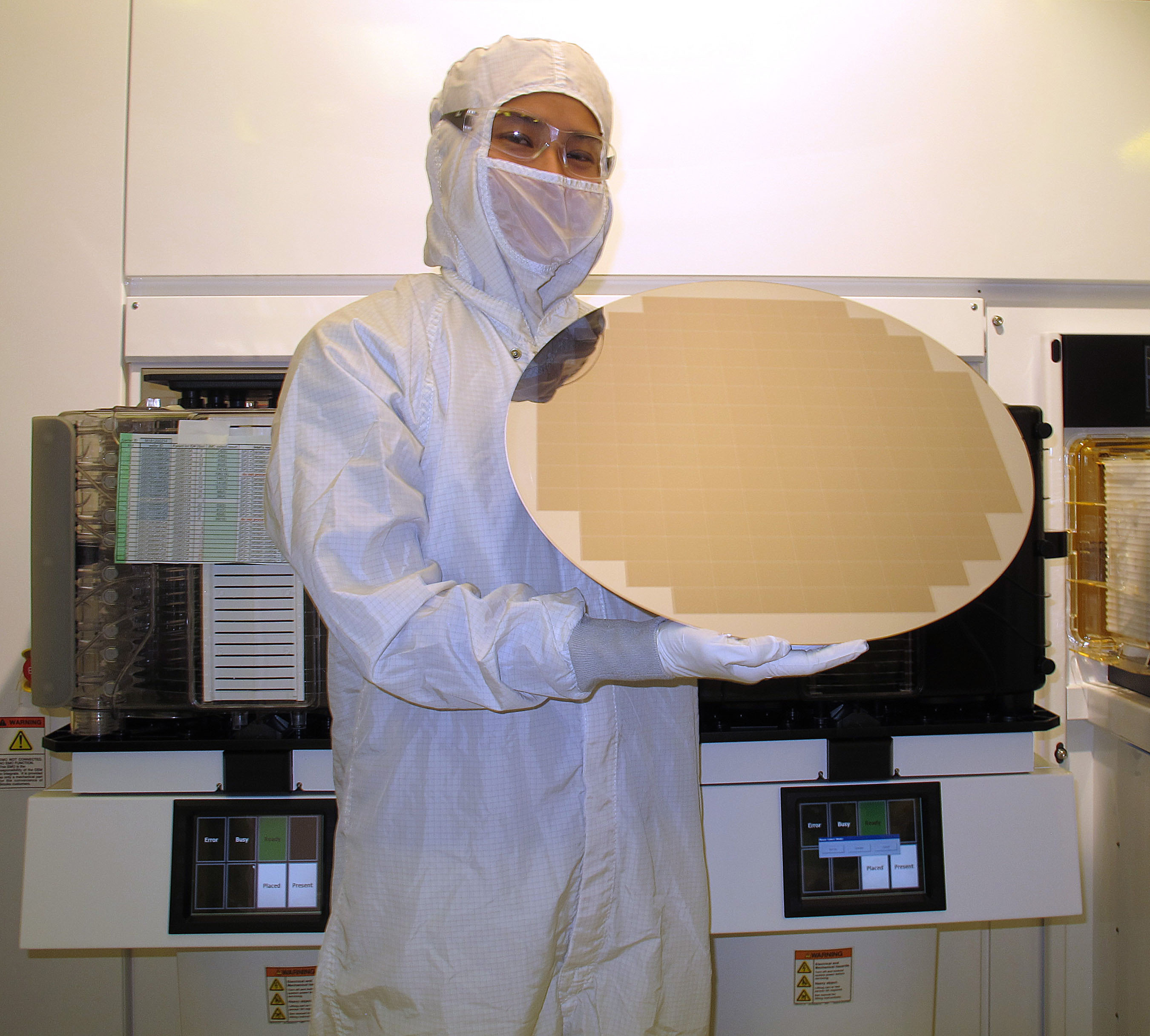
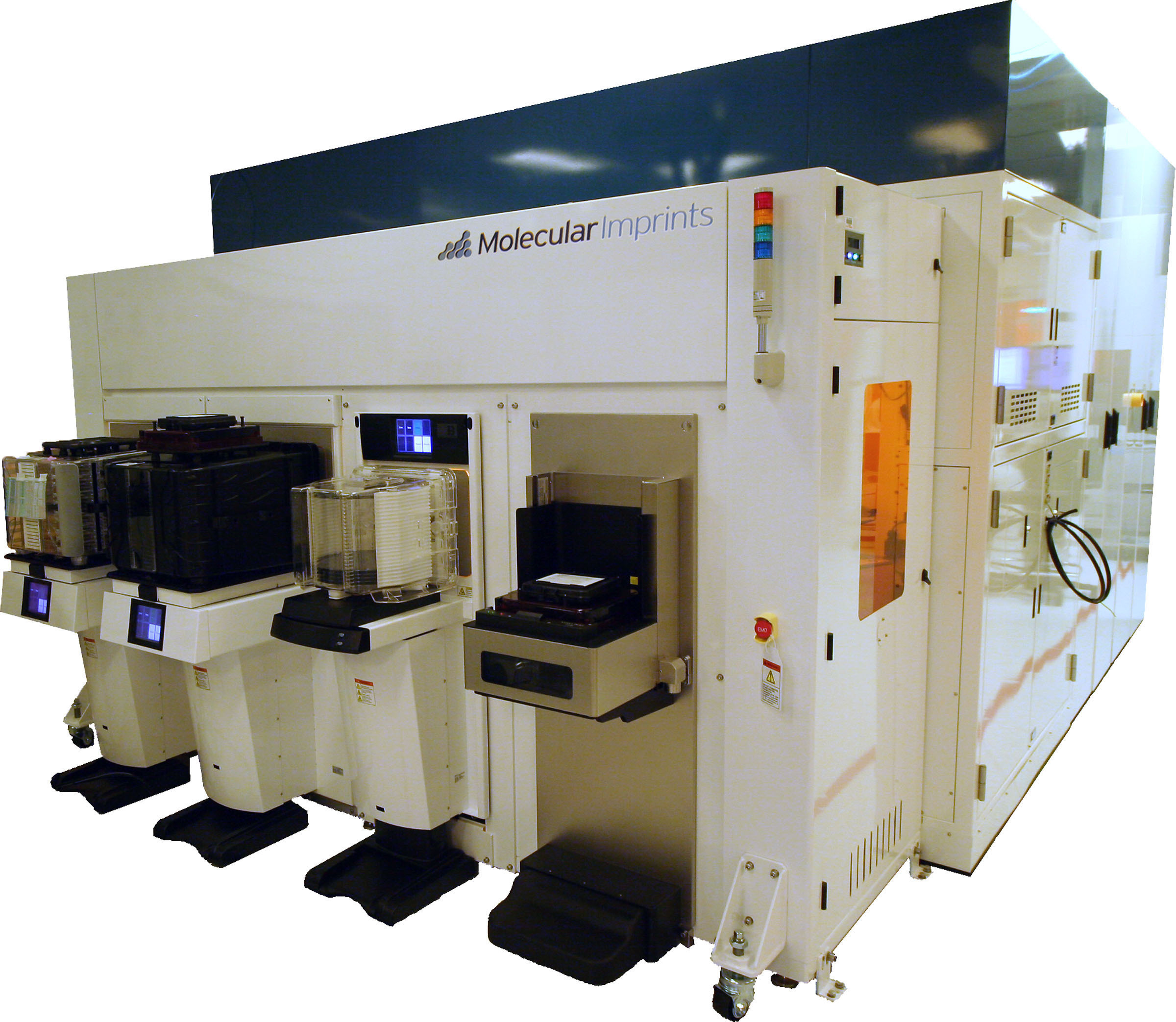
Using this lithography equipment called as Imprio 450mm, microprocessor chip giant Intel had drawn microscopic strands after strands of circuitry lines on a 450mm glass substrate and showcased a fully patterned 450mm wafers at SEMI’s Industry Strategy Symposium at Half Moon Bay, California on January 14th, 2013.

Added he, "Our proprietary Jet and Flash Imprint Lithography, or J-FIL technology is the only lithographic solution available today that can meet the demanding fine feature requirements of the industry's 450mm transition.”
J-FIL technology has demonstrated 24nm patterning with exceptional line edge roughness (<2nm LER, 3 sigma) and critical dimension uniformity (1.2nm CDU, 3 sigma) with extensibility to 10nm using a simple single patterning step process.
The Imprio 450 platform has a new stage and universal substrate chuck design that enables both 300mm and 450mm wafers to be processed without interruption.

As it comes with no complex optical lens and mirror, it is it well aligned with semiconductor memory manufacturing. This new 450mm patterning system acceptance coupled with our recent multiple module order announcement underscores Molecular Imprints tremendous progress towards placing J-FIL technology into high volume production of advanced CMOS devices.
Molecular Imprints, Inc. is a leader for high-resolution, low cost-of-ownership nanopatterning systems and solutions in the semiconductor, display and hard disk drive (HDD) industries. MII is leveraging its innovative Jet and Flash Imprint Lithography technology with IntelliJet material application to become the worldwide market and technology leader in high-volume patterning solutions for storage and memory devices, while enabling emerging markets in display, clean energy, biotechnology and other industries.

