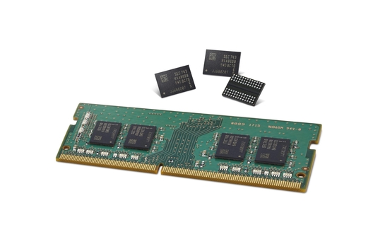
The mass production comes 21 months after Samsung started the first generation 10nm class circuitry 8Gb DRAM in February 2016.
Technology barrier to the 10nm circuitry process is so high that no other DRAM chip makers than Samsung have made to it using current immersion lithography technology.
They are now working on a next generation of EUV or extreme ultra violet lithography technology but the EUV technology is still in the field testing stage.
It will take a long while until it will be fully deployed in the mass production process.
The 2nd generation 10nm circuitry 8Gb DDR4 DRAM chip consumes 15% less power, but boasts of 10% more gains in the performances than the first generation 10nm circuitry products.
The new 8Gb DDR4 can operate at 3,600 megabits per second (Mbps) per pin, compared to 3,200 Mbps of the company’s 1x-nm 8Gb DDR4.
On the top of that, Samsung’s 2nd-generation 10nm-class 8Gb DDR4 features an approximate 30 percent productivity gain over the company’s 1st--generation 10nm-class 8Gb DDR4.
Technology innovation has enabled Samsung to make it to the 10nm-class circuitry mass production forgoing EUV.
Samsung has innovated on three technologies -ultra-high speed ultra-small, ultra energy efficiency circuitry technology, ultra sensitive cell data sensing technology, and air gap, or air spacer technology.
The newly devised data sensing system enables a more accurate estimation on where data is stored in each cell, which leads to a significant increase in the level of circuit integration and manufacturing productivity.
The new 10nm-class DRAM also makes use of a unique air spacer that has been placed around its bit lines to dramatically decrease parasitic capacitance. Use of the air spacer enables not only a higher level of scaling, but also rapid cell operation.
“By developing innovative technologies in DRAM circuit design and process, we have broken through what has been a major barrier for DRAM scalability,” said Gyoyoung Jin, president of Memory Business at Samsung Electronics. “Through a rapid ramp-up of the 2nd-generation 10nm-class DRAM, we will expand our overall 10nm-class DRAM production more aggressively, in order to accommodate strong market demand and continue to strengthen our business competitiveness.”
With these technology advancements, Samsung is now accelerating its plans for much faster introductions of next-generation DRAM chips and systems, including DDR5, HBM3, LPDDR5 and GDDR6, for use in enterprise servers, mobile devices, supercomputers, HPC systems and high-speed graphics cards.
Samsung has finished validating its 2nd-generation 10nm-class DDR4 modules with CPU manufacturers, and next plans to work closely with its global IT customers in the development of more efficient next-generation computing systems.

