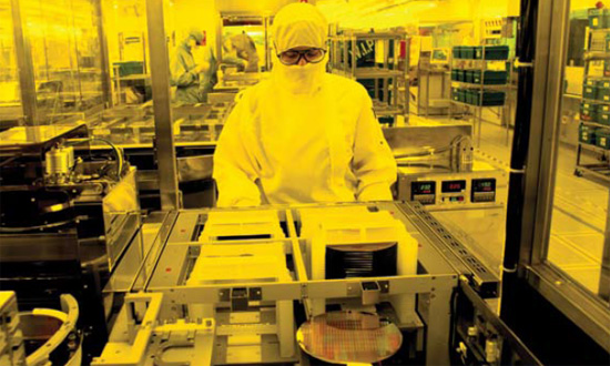
Known as the most advanced and finest chip circuitry technology so far, one generation behind EUV-based 7 node technology, the new 8LPP geometry technology delivers upfront of 10% lower power consumption and up to 10% silicon real estate reduction, compared with the predecessor 10LPP technology. The narrower circuitry node also translates into higher performances, allowing Samsung to address mobile, network, server applications as well as virtual currency like bit coins, which requires fast data processing.
The 8nm node technology is the latest and finest one after Samsung put 10nm node technology to commercial use in Oct, 2016 in a joint-effort with Qualcomm
The 8nm node technology was also commercialized in a technical tie with Qualcomm. The two chip maker’s cooperation began with a 14nm chip node technology development project.
“With the qualification completed three months ahead of schedule, we have commenced 8LPP production,” said Ryan Lee, vice president of foundry marketing at Samsung Electronics. “Samsung Foundry continues to expand its process portfolio in order to provide distinct competitive advantages and excellent manufacturability based on what our customers and the market require."
RK Chunduru, senior vice president of Qualcomm, said, “We have ramped up to the 8LPP ahead of original schedule, as we have used our proven 10nm process technology while providing better performance and scalability than current 10nm-based products.”
The recent update to the Korean chip maker’s foundry roadmap, including 8LPP availability and 7nm EUV development, will be presented at the Samsung Foundry Forum Europe held on October 18, 2017, in Munich, Germany.
The Samsung Foundry Forum was held in the U.S., Korea, and Japan earlier in the year.