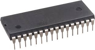
The implementation of the 7nm circuitry into SRAM marks an important technology milestone on the chip maker’s roadmap to 7nm application processor chips, as it lays out the foundation for attaining the 7nm circuitry cell on CPU chip.

For use in an on-chip cache memory, a temporary, built-in storage space on a CPU, the SRAM has almost the same cell structure as that of CPU, allowing chip makers to fabricate part of the chip as logic and part as SRAM memory. So, the implementation of 7nm circuitry SRAM represents one step closer to the 7nm-circuitry CPU or AP chip.
Almost one year after it had implemented a 10nm circuitry on a CPU, the chip maker started to produce 10nm circuitry APs in volumes in October.
The 7nm circuitry SRAM chip’s cell size is up to 32.5% smaller than its 10nm FinFET SRAM, consuming less power.
Unlike dynamic RAM (DRAM) that frequently refreshes electric charges at a certain interval not to lose bit data charged on a capacitor, SRAM stores bit data on a transistor, so doesn’t need to refresh them.

It is far faster in processing data than DRAM, as it cycles as fast as CPU, but building SRAM comes costlier, as it requires three times as many transistors for a given capacity as DRAM chip does.
Samsung will showcase the 7nm circuitry SRAM chip at ISSCC conference which to be held between Feb. 5 and 9, 2017 in San Francisco.
Samsung plans to demonstrate its newly developed a 4th generation 512Gb 64-layered TCL 3D NAND flash chip, boasting an input/output speed of up to 800Mbps. Mass production of the 64-layered 3D NAND flash memory chips will start in mid-2017 rolling out chips at a monthly capacity of 50,000 to 60,000 wafers in its Hwasung facility.

