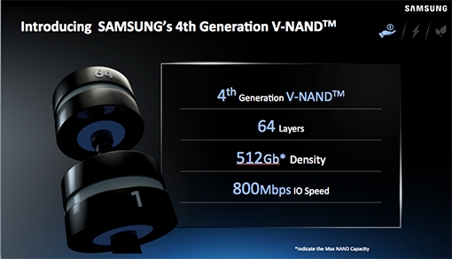
The 64-layer V-NAND flash memory chip is the latest of Samsung’s V-NAND lash memory chip line up following the rollout of a 24-, 32-and 48- layer NAND flash memory chips. Mass production of the 64-layer NAND flash memory chips will start in the fourth quarter of 2016.
Unlike a planar 2D NANA flash memory chips that lay out myriads of control and floating gates, and channels horizontally in a 2 dimension, the 3D V-NAND stack layers above layers of control gates in a cylindrical shape and then punches hole through the layers of control gates to the bottom. Coming next is to deposit non-conductive charge trap gates across the inside walls of the hole where a series of 1s and 0s bit data are stored.
1TB memory in a single BGA package
The vertical structure helps reduce cell interferences leading to the lengthening of the product life cycle. Coming to another advantage is the reduced costs per bit, as the vertical structure allows more of data to be stored in a given silicon space.
The cutback in costs is speeding up the penetration of NAND flash memory chips into SSD, or solid state drive market, as it allows SSDs to significantly narrow down the price gap with HDDs.
For example, Samsung’s latest Serial Attached SCSI (SAS) SSD is the world largest single drive ever introduced to the industry based on 512-gigabit (Gb) V-NAND chips. A total of 512 V-NAND chips are stacked in 16 layers to form a 1-terabyte (TB) package and the 32-terabyte (TB) SSD contains 32 of those packages.
The Samsung 1TB BGA SSD features an extremely compact, ball grid array (BGA) package design that contains all essential SSD components including triple-level-cell V-NAND flash chips, LPDDR4 mobile DRAM and a state-of-the-art Samsung controller.
It will deliver unprecedented performance, reading sequentially at 1,500MB/s and writing sequentially at 900MB/s. By reducing its size up to 50% compared to its predecessor, the SSD weighs only about one gram (less than half the weight of a U.S. dime), making it ideal for ultra-compact next generation notebooks, tablets and convertibles.
Next year, Samsung plans to launch its 1TB BGA SSD by adopting a high-density packaging technology called “FO-PLP (Fan-out Panel Level Packaging)” which Samsung Electronics developed with Samsung Electro-Mechanics.
New ‘Z- SSD’ breaks through performance limits
Samsung has also developed a high performance, ultra-low latency SSD solution, the Z-SSD. Samsung’s Z-SSD shares the fundamental structure of V-NAND and has a unique circuit design and controller that can maximize performance, with four times faster latency and 1.6 times better sequential reading than the Samsung PM963 NVMe SSD.
The Z-SSD will be used in systems that deal with extremely intensive real-time analysis as well as extending high performance to all types of workloads. It is expected to be released next year.