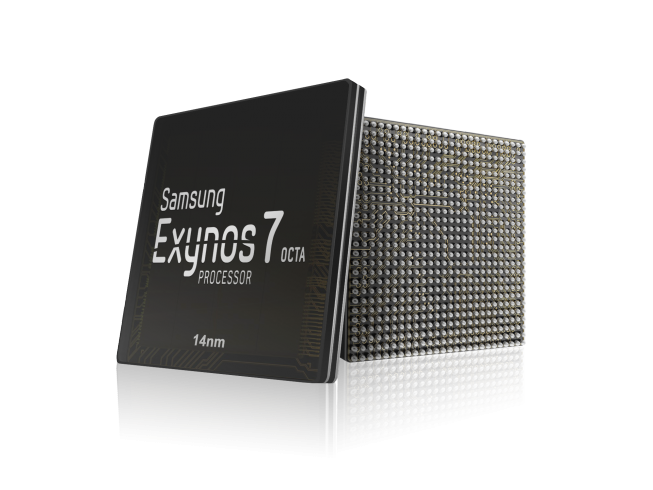
(iTers News) - Samsung Electronics Co., Ltd. said today that it has started mass production of a 14-nanometer, or nm FinFET process technology in what the chip maker said is the world’s finest 3D transistor structure ever.
To be used to produce its Exynos 7 octa-core mobile SoC platform, the 14nm 3D FinFET is what Samsung expects to help snatch back a foundry chip-making order for Apple from Taiwanese foundry chip maker TSMC.
“Samsung’s advanced 14nm FinFET process technology is undoubtedly the most advanced logic process technology in the industry,” said Gabsoo Han, executive vice president of sales & marketing, System LSI Business, Samsung Electronics. “We expect the production of our 14nm mobile application processor to positively impact the growth of the mobile industry by enabling further performance improvements for cutting-edge smartphones.”
TSMC outbid Samsung ’in the competition for seizing the foundry chip-making contract with Apple Inc. 2 years ago, as the Korean chip maker wrestled with its ramp up plan to produce a 20nm-class HKMG, or high-k metal gate process technology, but only to suffer low yield as well as many glitches.
To snatch back the order, Samsung skipped the high-K metal gate technology and went straight to the 3D FinFET technology.
Both of the HKMG and 3D FinFET technologies were to tackle fundamental technological challenges facing the chip-making industry, as the industry was struggling to fix up excessive heat leakages in their ramp-up plan to get a 20nm-class chip processing technology. Yet, HKMG is a sort of continuous innovation in the conventional 2D planar chip process technology, but the 3D FinFET is a disruptive, discontinuous innovation.
As the width of the transistor gate got below 20nm-class, the thickness of the gate insulator got too thin and too frail to stabilize the flow of electrons, resulting in electrons leaking out of the path or channel and generating heats. The heat generation translates into power waste. Worse yet, the width of the gate is so thin that it had a side effect of electron flowing even when voltage input was shut off in what’s called as static heat leakages in the industry’s jargon.
The HKMG technology is to deposit high-k materials, of which dielectric constant value is higher than k value, the standard dielectric value of silicon dioxide, a conventional material for the layer of gate insulator, instead of silicon dioxide, because the it has a natural property to hold electrons more tightly.
Yet, as the industry got below the 20nm design rule, the HKMG technology proved futile. This explains why the industry started to build the transistors in a 3D structure.
Unlike the planar structure transistor, the 3D FInFET technology allows the chip maker to stack transistors in the 3D structure like a fin keel that has multiple electron channels. The 3D structure allows electrons to move faster, while consuming less power.
TSMC has successfully taped out its own 16nm FinFET technology and is known to sign a foundry chip making contract with approximately 60 fabless chipmakers to churn out their chips using its own home-grown 16nm FinFET technology.
As the most advanced technology available today, Samsung’s 14nm FinFET process is able to achieve the highest levels of efficiency, performance and productivity. When compared to Samsung’s 20nm process technology, this newest process enables up to 20% faster speed, consumes 35% less power consumption, and allows the chip maker to get 30% more chips out of silicon wafer.
Samsung will build and mass-produce its next generation of Exynos 7 octa-core mobile SoC using this 14nm 3D FinFET process technology.


