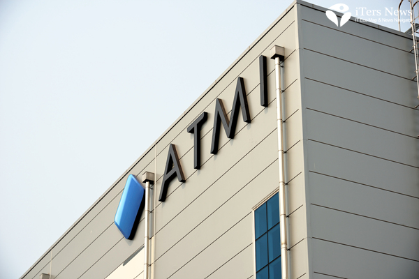
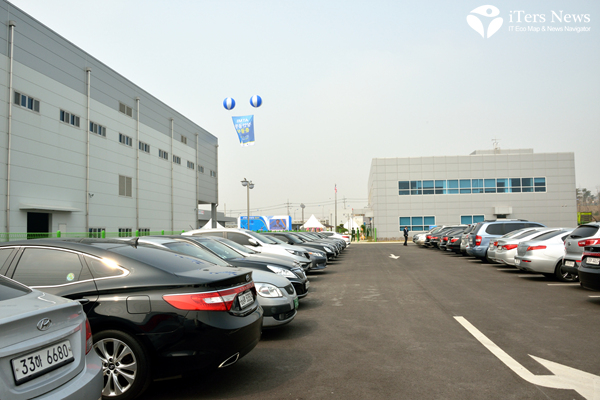
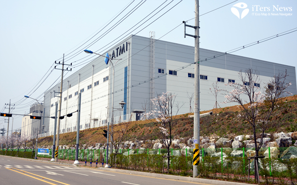
(iTers News) - Ion implantation chemical materials and delivery system maker ATMI of the U.S. has started the operation of its factory in Korea to produce an array of chemical materials for chip-making as well as toxic gas delivery and storage equipment. Spreading over a land lot of 25,891 square meters in the Jangan industrial complex in the city of Hwasung, Gyeongi province, the factory costs US$23.3 million to build. The investment amount is part of ATMI’s long-term investment spree to invest US$30 million in total through 2016 to position the Korean production facility as an export hub to serve Asian customers in China, Taiwan, and Southeast Asian countries.
More than 70% of a ATM’Is revenue comes from Asian regions, world’s biggest concentration of front-end wafer fabrication facilities. The Jangan factory will also supply world‘s two largest memory chip makers –Samsung Electronics and SK Hynix, Inc.- with an array of gasified toxic chemicals for ion implantation like baron and phosphor as well as gas delivery and storage system and equipment. The company is also supplying LG Display Inc. with a chemical packaging system for display panel fabrication.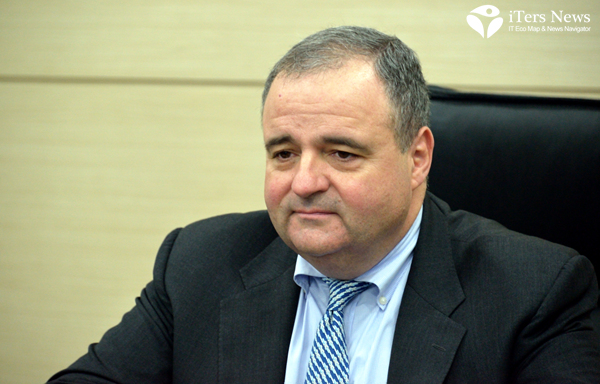
At a tape-cutting ceremony for the opening of the facility, Christian Kramer, senior vice president, Microelectronics with ATMI, said, “When we look at the places in the world for the semiconductor industry, that truly matters, that have truly growth opportunities , Korea comes right on top of the list. We have also key customer here in Korea both for ICs and displays. That couples with tremendously capable workforce that will be able to leverage and increase our business worldwide.
“All these factors came together to make this Jangan facility a great place for our additional investments. One of the great aspects of this facility is that it is manufacturing. But we very focus on developments and on R&D here in Korea through our technology center here in Suwon. The goal of being here is to be able to develop new products and new capability in that facility, and then we can bring high level of manufacturing in this Jangan factory “ added he.
ATMI is also operating a R&D center in Suwon, Korea, closely working together with Samsung Electronics and SK Hynix to help or consult with them to develop new formulation for chemical compounds, as chipmakers are struggling to improve yield – the ratio of sellable items out of total production. The yield partly rests with the purity of the liquefied or gasified chemical compound.
The chemical gas and delivery system maker is supplying other chemical materials for ADI and CVD processes, too.
Ion implantation is one crucial part of a whole bunch of front-end chip-making processes where an array of toxic gases like baron phosphor, ash3 and ph3 are sprayed and showered to create tons of transistors and resistors in what’s called as CMOS or complementary metal oxide semiconductor process in the industry jargon.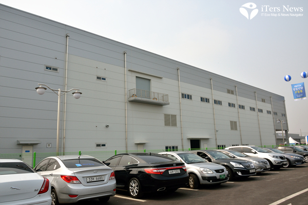
These gases like phosphor and boron compound are deposited to create P type transistors or N type transistors in a chemical reaction with silicon on a silicon wafer in a complementary manner.
ATMI’s toxic gas delivery canister like SDS is well known for its high-level safety feature, as it an extraction type. Toxic gases are tightly stored in a beehive-like carbonate sheet of ultra-tiny micro-holes so that no single drop of them is leaked out unless they are artificially extracted by force.
As semiconductor chip-making process goes below 20nm and beyond, chemical materials are increasingly more important than ever before, as its impurity can adversely affect the yield. The finer its design rule gets, the more of heat and electricity it dissipates, consumer more of current or voltages. So, chip makers are also increasingly require new chemical compounds or new chemical formulation to help reduce the heat dissipation.
Chemical materials like High-K are one of the newly formulated chemical compounds to reduce heat dissipation. The k is the value of dielectric constant. The high-k materials refer to materials of which its dielectric constant is higher than that of silicon dioxide, which is 3.9.
(Photos and Videos by JH Bae)