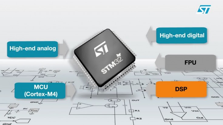
(iTers News) – STMicroelectronics unveiled the newest version of its STM32 MCU family – STM32 F3 series that integrate a high-performance ARM Cortex M4 MCU core and low-cost mixed signal analog components in a single silicon die.
Coming complete with an array of low-and middle-density on-chip memory and analog circuits like comparators, ADCs, DACs, Op amps, the F3 series of MUCs are specifically designed to address system designers’ strong requirements for price-competitive, but high performance MCU solution.
“Since we first introduced a mainstream STM32 F-1 series of MCUs in 2007, we have continued adding up the STM32 family, specifically mixing up ultra low-power LI, wireless connectivity-centric W, mainstream F1, and high-performance F2 and F4 series across applications ,“ said Choi, Kyung Hwa, marketing manager with STM Seoul office.
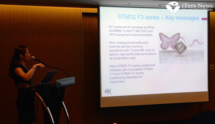
“By performance, the F3 series are positioned between high-end F4 series and mainstream F1 series to deliver on system designers’ ever increasing requirements for F4-like performance and F1 series’ cost-effective features,“ she added.
The F3 series of STM32 family are pin–compatible with FI and F4 series, allowing system designers to freely plug in and out them, depending on applications.
Catch two birds with one stone
According to marketing manager Choi, the STM32 MCU family is one of the most resilient MCUs in its chip portfolio, as it is the sort of a highly integrated cross-market MCU solution that can address as wide range of applications markets as possible.
The cross-market platform allows STM to offset setbacks in one application with sales gains in other applications.
As a result, unit shipments of STM32 family almost quadrupled even in 2009 and 2010 –one of the industry’s most tumultuous periods – for two years in a row. In fiscal 2011, unit shipments jumped 1.6 times year-on-year.
To keep the growth dynamics up and running, STM is staking out the F3 series as a new cost-effective alternative to the ultra high performance F4 series, which can match the performance of the F4, but comes at a relatively lower cost. .
The F3 series are built with the same ARM Cortex M4 MCU core that the F4 series are based on, sharing the same FPUs, or floating point units, but are operating at a clock speed of 72MHz, while the F4 series running at a frequency cycle of 168 MHz.
What stands out from the F4 series, too is that the F3 series are integrated with a wealth of mixed signal analog components, which otherwise would have been sit on a board as discrete components.
High integration
The high integration features translate into cost reductions and smaller form factors for system board designs.
In terms of performance, the F3 series stick out from other Cortex M3-based STM32 family peers, too.
For example, the F3 series are operating at the same clock speed of 72MHz as the mainstream F1 series run, but can process instruction sets at a speed of 95 DMIPS, or dhrystone million instructions per second, far faster than the F1 series’ 61 DMIPS.
STM’s proprietary 8-Kbyte CCM-SRAM, or core coupled memory-SRAM technology plays a key role in hype-driving the instruction sets.
The ARM Cortex M4 is built with what’s called as Harvard architecture, which has two separate bus interfaces between a CPU core and on-chip memory systems –I-bus, or instruction bus for codes, and D-bus for data.
As a set of codes are stored in non-volatile flash memory system, a CPU core always has to wait a number of cycles before they bring up codes out of its on-board flash memory system and process them.
That’s because the clock speed of the CPU are far faster than that of the flash memory system, resulting in data latency.
Hype-driving instruction sets
By putting the CCM-SRAM on I-bus and temporarily storing instructions sets on volatile SRAM for processing, STM tackled the speed mismatch, bringing up and processing them at the same clock cycle of 72MHz as that of the CPU core, said manager Choi
The math of CCM- SRAM operation is straightforward. Critical routines are loaded in CCM start-up and can be completed at full speed in zero wait state, achieving 95 DMIPS at a 72 MHz, and resulting in a 52 % speed improvement, compared with flash execution.
This is great of help for fast execution of critical routine executions such motor control and audio filtering.
The CCM-SRAM features are only available the high-end F30x line of STMF32 F3 series, and are a perfect fit for real time operations of a liner motor.
The CCM-SRAM can double as normal pure data SRAM, too.
The F3 series have also outstanding safety features, incorporating hardware SRAM parity check safety, memory protection unit, write-protection-cell, and clock security system, 2 independent watchdogs, and cyclic redundancy check.
The clock security system is a sort of back-up clock recovery system that switches the MCU to back-up internal RC in case of external clock failure of an external MCU.
The F3 series also incorporate an upfront of 256 Kbyte- on-chip flash memory circuits, up to 32Kbyte-RAM, Op amp with a built-in gain values with 1% accuracy, AMC, or advanced motor controller timer, and a high-speed 12 bit ADC of 5MSPS, or 5 mega samples per second.
The 12 bit ADC can convert analog signals into Os and 1s of digital data at a high-speed of 5MSPS. And, the ADC timer operates double the clock speed.
Such versatile and multi-faceted features of the F3 series are what make them a great fit for a wide range of applications markets.
Jack of all trades
For example, the F3 series can be used with a wide variety of home appliances and small –size consumer electronics products that are powered by an array of linear, miniature motors.
That’s because the F3 series incorporate advanced analog IPs like fast comparators, Op amps, and 12 bit ADC and DAC, which are good at dual motor control and power factor correction, or PFC. .
Consumer applications are another bet, as the F3 series incorporate USB 2.0 interface, CEC, and I²S interface for entry-level audio control.
Its built-in 16-bit sigma ACD is also a key built-in building block that makes the F3 series double as a biometric sensor.
As the digital domain of the F3 series operate at 1.8 volts, the same voltage level as applications processors, the brain of the smartphones and tablet PCs, it can be used with them, too. The analog domains operate at 3.6 volts
The F3 series can serve as a MCU for capacitive touch key or pad, as well, getting the controller load off the main system CPU.
Their application areas don’t stop there. The F3 series are good at digital power conversion for entry-level digital power supplies, solar inverters, LED lighting, and metering.
The two versions of the F3 series are now available in the market, including STM32F303VC and STM32F373VC.
The rest of the F3 series will be available in the 3rd quarter, including a 1.8V dedicated version and a wafer-level-chip scale package 66 pin version.


