(iTers News) – A growing bunch of smartphone users are downloading and playing back tons of graphics-rich and power-hungry 3D and full HD games, movies and apps more frequently than ever before, draining the battery power of their smartphones to limit.
To keep the power consumption to the minimum, CPU makers are aggressively exploring a new way of chip-designing, which will allow them to create a power-thriftier CPU, or applications processor chip.
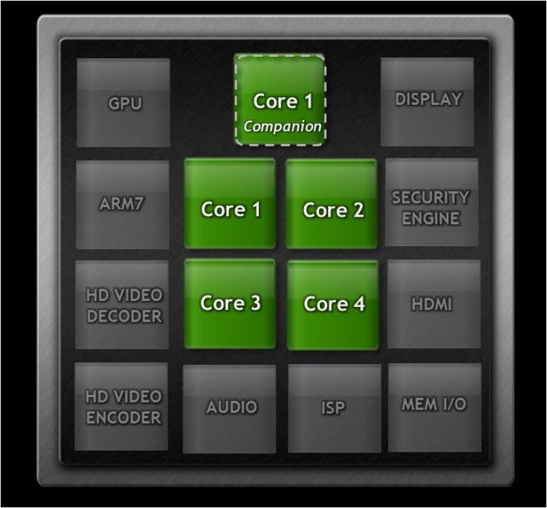
Cases in points are Qualcomm Inc. and Nvidia Ltd., both of which license microprocessor architecture IPs from ARM Holdings of the U.K and then build their own application processor SOC chips around the ARM processor cores. Nvidia has built its quad-core Tegra 3 applications processor chip around an ARM Cortex 9 processor core, but with a twist to save power. The Tegra 3 processor chip implemented a novel new variable symmetric multi-processing, or vSMP technology to have 4 main processor cores plus one more variable symmetric multiprocessing, or vSMP core packed on a single silicon die.
Called as a companion core, or a battery saver core, the vSMP core was built using a special low power silicon process that executes background, or low performance tasks –Email syncs, social media syncs and live wallpapers- at low frequency for active standby mode.
Meanwhile, the four main processor cores perform heavy and high frequency tasks like video playbacks and Web browsing, which are all happening at a time whenever users actively interact with their machines.
vSMP technology with a twist
“The 4 core-plus-one architecture is why Tegra 3 is different from other smartphone CPUs,” said Matt Wuebbling, director of product marketing for Tegra with Nvidia Ltd.
According to him, the beauty of Tegra 3 is its unique 4-plus-1 quad core CPU architecture that not only delivers outstanding performances, but also ensures big savings in battery life to deliver up to 5 times more performance than what Tegra 3, the world’s first dual core processor, performs.
Here is a magic of how four main cores and one companion core of the Tegra 3 CPU work together in sync to perform high frequency tasks like media playback and Web browsing faster, but with less power than the Tegra 2.
Trade-off
In theory, the power consumption of a CPU is usually a total sum of leakage power and dynamic power consumption. When a silicon device is operating at or near peak frequency, the total power consumption of the device is mainly determined by the dynamic power consumption. Meanwhile, the device is idle, or stay somewhere near idle, the leakage power takes up a significant portion of the total power consumption.
Whenever chip makers are trying to scale down its silicon process technology, or design rule to have a SOC chip perform better and faster, but consume less power, the major technological challenge facing them is how to cut back on leakage power consumption.
That’s because the narrower the width of the silicon gate is, the more of leakage power is consumed under idle or active standby mode, generating more of heat. On the contrary, the CPU cores, or transistors of the smaller gate geometry consume less of the dynamic power, because the cores don't require abrupt increases in operating voltages when they switch from active standby, or idle mode to high-frequency ranges
When the CPU cores or transistors are built with the wider design rule, or gate geometry technology, however, the opposite is true of the power consumption. For example, they do consume less of leakage power, but more of dynamic power, because it sparks off sudden and big jumps in the power to wake up the transistors from active standby, or idle mode.
The so-called nanometer design technology such as 45nm or 30nm is called after the width of a gate of a transistor. The narrower the width of gate is, the faster it can process data.
Smart workload management
Nvidia’s vSMP technology takes advantages of only the merits of the faster and slower design rule technologies, allowing the chipmaker to build the high-frequency and performance-hungry main cores on a finer design rule, while fabricating the low-power and low-leakage companion core with less advanced slower design technology.
At the heart of the vSMP technology is also its dynamic voltage and frequency scaling (DVFS) and CPU Hot-Plug management software. The software set can intelligently manage the switch back and force of workload distribution between the main cores and the companion core based on applications and operating system requirements.
“For instance, if you are just holding a screen, the touch algorithm is running on a companion battery save core waiting for next action on a very low power idle mode, while the main four performance core is off. Once you take a next action to interact with your device by touching a screen to play games, for example, your battery save companion core is turned off. But all of OS processing as well as touch processing job transfer onto the performance core that get into action to perform high-frequency and fast-speed jobs, “added director Matt Wuebbling.
According to him, vSMP technology not only delivers ultra-low power consumption in active standby states, but also on-demand peak quad core performance for performance-hungry applications such as gaming, Web browsing, and flash media, and video conferencing.
The Tegra 3 CPU is now powering up an array of smartphones and tablet PCs, including HTC 1X, LG 4X HD Optimus 2, Toshiba 7.7-inch and 13.3-inch tablet PCs, Asus Transformer Pad, ZTE 7-inch and 10-inch tablet PCs
Two cores operate asynchronously

Qualcomm Inc. also introduced asynchronous CPU chip architecture, which is implemented on a line of its Snapdragon chip solutions, especially Snapdragon S3 and S4 processors. As the naming suggests, the asynchronous architecture allows individual cores on its Snapdragon processor, whether they are dual or quad, to operate asynchronously on different frequencies, or different voltages, depending on what they perform.
Compared with a synchronous architecture, according to Qualcomm, the asynchronous architecture is 30% to 40% more power-efficient, as its own built-in software algorithm assigns the CPU to process low-frequency background tasks on low voltage-powered processor core.
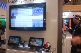
“One of the main characteristics of Snapdragon processor is that we have what we call as asynchronous operation of the multi-cores. This device, for example, shows there are two cores –core 0 and core 1, which shows dual core processor, a Snapdragon S4-class dual core processor,” said Takayuki (Ted) Nozaki, senior director of business development with Qualcomm Japan Inc.
Added he, “You can see two cores here. Because this is asynchronous architecture, core one is running in this way (in action), but core two is sleeping idle. And in terms of clock frequency of each core, because this is only running and up right now, this is virtually sleeping. With that, we are showing this is going to be more efficient in terms of power saving, compared with synchronous dual core operations which are supplied by other chipset manufacturers (suppliers).”
Advantages outplay challenges
According to him, Qualcomm is the only company to design this asynchronous operation of multi-core system from scratch. Although this is based on standard ARM core that doesn’t support this architecture, Qualcomm has its own algorithm and design way to have these two cores work in asynchronous way, consuming different level of voltages.
Thermal management is another advantage of the asynchronous architecture.
At the center of this asynchronous is also a software firmware that can manage system workflows between individual cores of different voltage supplies, depending on jobs which they should perform.
To make this asynchronous system work, Qualcomm faced a touch technological challenge of fabricating individual cores on different voltage design rules.
“Take a quad core CPU for example. We have to have four different voltage circuitries. This could be big challenge for us, but the advantage (of lower power consumption and less heat generation), which we can get from this architecture, prevails over challenges,” said Ted Nozaki.
What makes differences between Nvidia’s vSMP technology and Qualcomm’s asynchronous architecture is that Nvidia’s vSMP companion core is OS software-transparent, which means that OS and applications are not aware of this core, but automatically take advantage of it. This OS transparent architecture is known to save significant software efforts and new coding requirement.


