Choi Taewon, CEO of SK Hynix, was quoted as saying, “How SK Hynix will technologically fare in the competition with rivals both at home and abroad rests with the competitiveness of domestic semiconductor materials and equipment makers. This is the reason why SK Hynix is now strengthening its technology tie-up with our major ecosystem partners to finally and technologically help them to develop new equipment and new raw materials.”
His comments come at a time when the global chipmakers are facing tough technology challenges in ramping up to 20 nm and below geometry technology for DRAM chips ss well as 64 layer 3D NAND flash memory chips. All the challenges have more to do with the way of how to compound new raw materials than equipment itself.
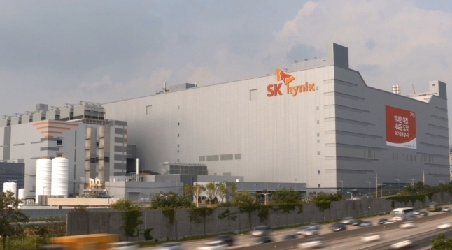
The program is part of the chipmaker’s long-term effort to help the county to localize key semiconductor materials and front-end equipment to lessen its heavy dependence on foreign equipment makers.
Under the financial and technological aid program, SK Hynix will sort out dozens of ecosystem partners not only to finance their technology development projects, but also guarantee minimum purchase of their newly developed equipment and materials.
As the first phase of the program, about 15 start-ups were singled out as the beneficiary of the program.

Among them are APTC, Auros Technology, and Ntrium, to name just three.
APTC is a chip etching equipment maker. As the market is near-dominated by Lam Research, the successful development and growth of the company will likely help SK Hynix in buying etching equipment at a cheaper price.
Auros Technology is a company that successfully has localized overlay inspection equipment. KLA-Tenkor is currently maintaining its near-monopoly in the market.
Ntrium is currently developing ink-type electromagnetic interference or EMI shielding material. It will be the first ink-type EMI shielding material ever developed locally, opening the way for commercializing spray-type EMI shielding process replacing current sputtering process.
It will help reduce the cost and increase the productivity.