At a technology roadmap seminar for future, discontinuous chip and display panel fabrication held in Seoul, top-level, senior engineers of Korea stressed that developing new, novel, high performance raw materials will become more crucial and effective than ramping up to new chip and display fabrication technologies in tackling emerging technology challenges
As the chip circuitry patterning technology moves closer to 10nm geometry, for example, so is the size of capacitors and transistors in memory chips. That progressively smaller transistor poses biggest technical challenges to chip makers, forcing them to hurry to find new chemical materials of high dielectric property .
That’s because the narrower the distance between source and drain of a transistor gets, the more likely electron veers out of course between them, dissipating heat and then consuming more power.
Especially, the power and heat leakage gets increasingly difficult to control, as the width of the chip circuitry gets down to 10nm geometry level and below.
To tackle these tough challenges, chipmakers in Korea are looking for other dielectric chemical materials than today’s mainstream Zr or zirconium, of which dielectric constant are higher than that of Zr.
Replacing SiO2 or silicon dioxide, Zr has been widely used as dielectric materials to etch capacitors of DRAM chip, where electronic charge, or voltages are applied to store data.
Hong Jong Seo, executive director of semiconductor R&D center at Samsung Electronics, said “Zr-based materials have been used in the DRAM chip fabrication till so far, but materials of high higher dielectric constant needs to be developed to achieve 10nm and below circuitry.“
Echoing his view, Lee Byung Kee, executive director of future technology development institute at SK Hynix, said “Developing new materials is the shortcut to technology innovation, because we don’t need to invest to develop new equipment or fabrication processes, which take long-time and is prohibitively expensive.”
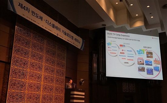
The same is true of display panel fabrication, as panel makers are struggling with blue LED chips to create true RGB OLED panels.
Red, green, and blue organic materials are composed to make OLED cells. While red and green are phosphorescent materials, blue is fluorescent material.
As phosphorescent material offer more rich-color and is power-efficient, blue phosphorescent material needs to be developed to further improve the OLED performance.
Lee Jong Hyuk, executive director of display R&D center at Samsung Display, said “Blue phosphorescent material needs to be developed to make power-efficient, life-like picture OLED display.”
Yoon Soo Young, executive director of R&D center at LG Display, said “Like the organic materials, film materials also needs to be researched for future displays like bend-able, roll-able and flexible display.”