In my previous blog post, I provided a review of the overall power device market and trends driving changes in device evolution that entail materials innovation. For the industry to make such a shift, the advantages over mature, low-cost silicon technologies must be compelling and something the industry absolutely has to implement. Now I’d like to focus on new materials offering competitive benefits over silicon in a growing number of power device applications.
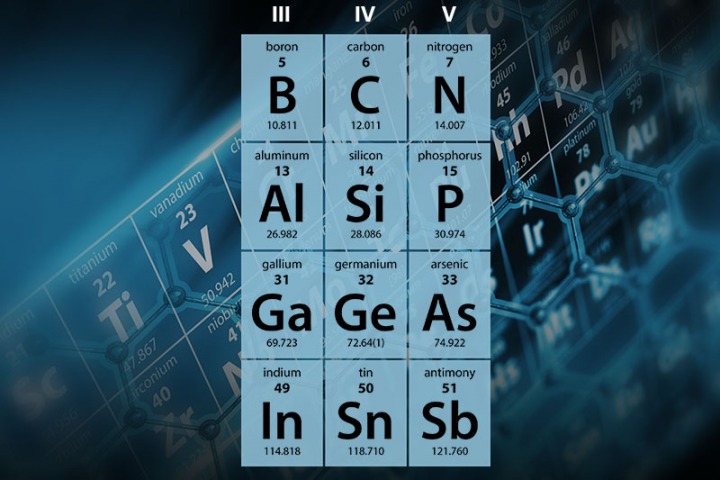
Silicon carbide (SiC) and gallium nitride (GaN) are the two materials undergoing early stages of adoption to improve power device performance. They are compound semiconductor materials which belong to the lll-V class of materials and offer wide bandgap (WBG) properties capable of taking power device performance to a level where silicon simply cannot compete. This is because WBG materials permit devices to operate at much higher voltages, frequencies and temperatures than conventional semiconductor materials like silicon.
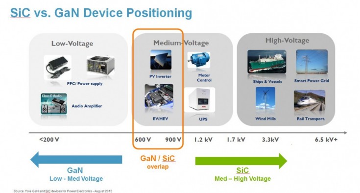
Figure 1. Wide bandgap power devices have advantages for numerous applications, but manufacturing processes are a challenge. (Source: Yole Development)
The challenge with these WBG lll-V substrates is they’re extremely expensive and difficult to manufacture. Compared to Si substrates, GaN substrates are generally 6 inches or smaller, some are 8 inches but supply is quite limited. SiC substrates are just entering 6 inches now. Wafer bowing and defects are key challenges the industry has yet to overcome. A 4-inch SiC substrate suitable for FET type power device fabrication can easily cost in the thousands of dollars range. Even with savings in energy and reduction in weight, size and circuit components, that’s still a large cost delta for makers of end-user products to justify. And then there are also reliability concerns.
Among the post-Epi process challenges is the need for super-high temperature anneals, reaching as high as 2,000°C. Typical anneal reactors for Si come nowhere near this regime. Implanting into SiC also requires high temperatures and is quite complex. For GaN, aluminum nitride (AlN)-type buffer layers are required due to the lattice mismatch between GaN and Si. These buffer layers are non-trivial and require tuning to help minimize charge traps. In addition, GaN on Si power devices are normally ON, which introduces reliability issues and further limits market acceptance. Enhancement-mode GaN devices would be needed to overcome this shortcoming. As for GaN on GaN, only 2-inch wafers are available today so it’s even more cost prohibitive.
Fortunately, other steps in the semiconductor processing flow, such as CVD, PVD, etch and CMP are relatively straightforward for WBG power devices. Also favorable is the process flow is very similar to that of silicon. Process tuning is required along with minor hardware changes, but existing technologies can be adapted to WBG processing.
Today, SiC and GaN products are available, albeit in limited quantities. GaN-based power devices are being used primarily for low- to medium-voltage applications, and SiC for medium- to high-voltage applications. While the performance benefits are undeniable, it is an open question whether WBG devices can overcome the cost and manufacturing challenges and achieve high volumes.
With the exciting potential of WBG devices, several companies, consortia and university research centers are focused on solving WBG power device challenges. Although costs must come down significantly before the benefits of WBG – including power savings, simplified circuitry and reduction in module size — can provide a meaningful return on investment compared with silicon substrates, these materials are still widely considered the next big inflection for the future of power devices.
- Ben Lee -